 Abayomi T. Oluwabi1*
 Nicolae Spalatu1*
 Natalia Maticiuc2Atanas Katerski1Arvo Mere1Malle Krunks1Ilona Oja Acik1
- 1Laboratory of Thin Film Chemical Technologies, Department of Materials and Environmental Technology, Tallinn University of Technology, Tallinn, Estonia
- 2Competence Centre Photovoltaics Berlin (PVcomB), Helmholtz-Zentrum Berlin für Materialen und Energie, Berlin, Germany
The deposition of nickel oxide (NiOx) thin film from an acetylacetonate source using many solution-based techniques has been avoided owing to its poor solubility in alcohol solvents. From this perspective, this work provides a systematic investigation of the development of NiOx thin film, using a combinative approach of ultrasonic spray pyrolysis (USP) and Li dopant for the synthesis and optimization of structural and optoelectronic properties of the films. An in-depth comparative analysis of nickel acetylacetonate-based precursor, employing acetonitrile and methanol as solvents, is provided. It is demonstrated that USP from acetylacetonate precursor yielded uniform, well-compact, and transparent films, with polycrystalline cubic NiOx crystal structures. By screening the deposition temperature in the range of 300–450°C, a temperature of 400°C was identified as an optimal processing temperature leading to uniform, compact, highly transparent, and p-type conductive films. At optimized deposition conditions (400°C), lithium-doped NiOx (Li:NiOx) thin film was deposited. The shift of the main (200) XRD peak position from 43.48° (0-Li:NiOx) to 43.56° (60-Li:NiOx) indicated Li incorporation into the NiOx lattice. An X-ray photoelectron spectroscopy (XPS) study was employed to unravel the incorporation of Li into the deposited Li:NiOx thin films. With the deconvolution of the Ni 2p core level for the as-deposited (0, 60)-Li:NiOx films, the intensity of Ni3+ related peak was found to increase slightly with Li doping. Furthermore, all the deposited Li:NiOx thin films showed p-type conductivity behavior, and the resistivity was reduced from 104 Ωcm (0-Li:NiOx) to 102 Ωcm (60-Li:NiOx). Based on these results, the deposited NiOx and Li:NiOx thin films suggested that USP-deposited Li:NiOx is highly suitable for application in inverted structure solar cells as the hole transport layer.
1 Introduction
Nickel oxide (NiO) is one of the few stable and transparent transition metal oxides, and it has a wide optical bandgap (Eg > 3.60 eV) and p-type electrical conductivity (Caruge et al., 2006; Napari et al., 2020). Due to these fascinating optical and electrical properties, numerous attempts have been made to integrate NiOx thin films into various electronic and optoelectronic devices (Ohta et al., 2003a; Ohta et al., 2003b). Mesoscopic NiOx thin films, for instance, have been widely employed as an electrochromic material for smart windows (Sato et al., 1993), an electroactive material for batteries or supercapacitors (Goodenough et al., 1958), and a photocathode for dye-sensitized photo-electrochemical cells (Zhang et al., 2016). In addition, owing to their p-type conductivity, nanocrystalline NiOx thin films have recently gained enormous interest as electron barrier layers in light-emitting diodes and organic/inorganic photovoltaic devices (Irwin et al., 2008; Jeng et al., 2014). However, the development of NiOx thin film has faced many challenges because, in the electronic structure of the p-type NiOx semiconductor, the O 2p orbital is naturally localized in the valence band (VB), which makes the introduction of shallow acceptors challenging. Hence, undoped NiOx thin film has been widely reported to be electrically resistive (1013 Ω cm) at room temperature (Barquinha et al., 2012; Krunks et al., 2014).
The electrical performance of NiOx thin films can mainly be improved by inducing more Ni vacancies and forming interstitial oxygen within the bulk of NiO crystals. To achieve this, several groups have tried doping NiOx with monovalent Li+ ions or co-doping with Mg2+ ions, assuming that each Li+ ion donates one hole to the top of the VB in order to keep charge neutrality (Sato et al., 1993; Krunks et al., 2014). In the literature, there is a wide discrepancy regarding the hole mobility and conduction mechanisms of NiOx (Zhang et al., 2018). Guo et al. (Guo et al., 2013), for instance, reported a reduction in the resistivity of nanocrystalline Li:NiOx thin film to ∼ 103 Ωcm as a result of increasing the concentration of Li atoms in the precursor solution. (Chen et al., 2012), on the other hand, were able to achieve a lower resistivity of ∼ 0.02 Ωcm by doping NiOx with copper (Cu). Doping was also reported to improve the crystallinity and the transparency of the NiOx thin films (Chen et al., 2012). Alver et al. reported a decrease in the transparency of NiOx thin film by introducing B3+ impurities into the NiOx thin film (Alver et al., 2013) and an increase in transparency by doping with Li (CHEN et al., 2012).
For the deposition of NiOx thin films, several physical (Sato et al., 1993; Ohta et al., 2003a; Pan et al., 2019) and chemical (Ohta et al., 2003b; Chen et al., 2021) (https://www.sciencedirect.com/science/article/pii/S0042207X14000657?via=ihub) methods have been employed, including chemical vapor deposition (CVD) (W Han et al., 2016), sputtering (Ohta et al., 2003a; Pan et al., 2019), atomic layer deposition (ALD) (Napari et al., 2020), sol-gel spin coating, chemical bath deposition (CBD) (Xia et al., 2008), electrodeposition, and ultrasonic spray pyrolysis (USP). The feasibility of all these deposition techniques has been proven for the synthesis of NiO, as well as for other functional oxides and a larger extent of the application range (Yu et al., 2022a; Yu et al., 2022b) (Yu et al., 2014). Among the various methods, USP has several advantages, such as low-cost, simplicity, offering the possibility of depositing uniform thin film over a large area, and ease of scaling for industrial applications (Oluwabi et al., 2020; Eensalu et al., 2022). One of the most important advantages of USP is a high degree of freedom in the choice of mixing the precursor solution (Wu and Yang, 2013; Krunks et al., 2014). In the literature, USP has been reported as a deposition method for charge transport layers (TiO2 or NiO) in dye-sensitized solar cells (Chan et al., 2011; Eensalu et al., 2019). Moreover, USP-deposited TiO2 has recently been employed as a heterojunction partnering layer in antimony chalcogenide-based solar cells (Eensalu et al., 2022; Koltsov et al., 2022). Compared with the n-type TiO2 electron transport layer (ETL), USP-deposited p-type NiO films can be used as an electron barrier layer in similar chalcogenide-based single and tandem solar cells (Napari et al., 2020; Eensalu et al., 2022). In perovskite-chalcogenide tandem cells, for instance, NiOx seems to be a good companion for organic hole transport layers (HTLs). For this application, expensive physical methods have been reported for the deposition of NiOx, which are limited by poor coverage of the rough surface of the underlying chalcogenide absorber (Jošt et al., 2019). Our recent study on the development of ZnO nanorod/NiOx core-shell structures demonstrated that conformal uniform coverage of NiOx with a thickness of some nanometers could be deposited by USP on ZnO nanorods (Chen et al., 2022). Therefore, USP-processed NiOx thin film could be an excellent approach to solve this problem. However, a low processing temperature ca 200°C is required in order to be compatible with perovskite and emerging chalcogenide thin film solar cells (Juneja et al., 2022) (Krautmann et al., 2023).
Nickel chloride (Krunks et al., 2014), nitrate (Joseph et al., 2008; Tenent et al., 2010; Juybari et al., 2011), acetate (Desai et al., 2006), and acetylacetonate (Chan et al., 2011) are common precursors used to deposit NiOx thin film via the spray pyrolysis method. The suitability of these precursors has been reported by different research groups. In the case of chloride and acetate salts, in our previous report (Krunks et al., 2014), we comparatively studied the structure and morphological changes in spray-deposited p-type NiOx thin film from aqueous and alcoholic solutions of nickel chloride and nickel acetate. We reported that the difference in the thermal decomposition of the chloride or acetate precursor salts was crucial in the formation of sprayed NiOx thin film and led to changes in the film’s microstructures. Similarly, Kamal et al. (Kamal et al., 2004) reported a porous NiOx thin film deposited from chloride precursor salts by spray, and a traceable amount of chlorine residue. In the case of the nitrate precursor route, the stability of the precursor was still uncertain during the decomposition process. On the other hand, Gomaa et al. (Gomaa et al., 2017) showed that the optical transparency of NiOx thin film could be enhanced when deposited from nitrate precursor.
The deposition of nickel oxide (NiOx) thin film from an acetylacetonate route has been an avoided precursor source for many solution-based techniques owing to its poor solubility in alcohol solvents. In addition, acetylacetonate is a coordinating ligand with two bidentate organic moieties that enhances the chelating complex that dissolves poorly at room temperature in alcohol (Williams et al., 2001). This has discouraged the use of acetylacetonate precursor by solution-based deposition methods such as spin coating. The great uniqueness of this work was to show that ultrasonic spray pyrolysis (USP) could be used to deposit a uniform, transparent, NiOx thin film with fine grain structure without any drawback in terms of performance when compared with spin coating, which is a common technique used to deposit NiOx from solutions. We provide for the first time a systematic comparative study of the development of NiOx by USP, using acetonitrile and methanol as solvents in the precursor. Furthermore, this solution processing is combined with a Li doping approach to develop p-type NiO thin films with enhanced electrical properties. We aim to optimize the deposition of NiOx thin film using these solvents, and to describe the effect of Li alloying in the solution of NiOx on the structural and electrical properties of NiOx thin film.
2 Experimental procedure
2.1 Precursor solution preparation
The NiOx precursor solution was synthesised by dissolving nickel acetylacetonate (Ni(C5H7O2)2); Sigma Aldrich, 98%) in methanol (Me-OH, CH3OH; Honeywell, 99.8%) and acetonitrile (ACN, C2H3N; Honeywell, 99.9%) at room temperature to yield a solution whose Ni2+ ion concentration was equivalent to 2 mmol of solute in 100 mL. The solution was stirred for ∼ 30 min to ensure homogenous dissolution of solute into the solvent, which was completely transparent with a green colouration. All the reagents used were HPLC-graded, therefore there was no reason to further purify them.
Lithium nitrate (LiNO3) [99%; Alfa Aesar] salt was employed as the Li dopant source. The Li:NiOx solution was synthesised by mixing a quantitative amount LiNO3 salt with Ni(C5H7O2)2 salt in methanol, and the [Li]/[Ni] mol ratio in solution was varied from 0 to 60 mol%.
2.2 Thin film deposition and post deposition treatment
Before the thin film deposition process, all the borosilicate glass and quartz substrates were ultrasonically cleaned at 60°C in acetone, ethanol, and distilled water for 10 min in respective order, and later air-dried. To optimize the NiOx thin film deposition, the films were deposited via the ultrasonic spray pyrolysis (USP) method at different deposition conditions, such as temperature (Ts) being varied from Ts of 300–450°C. The process and the technique involved with the USP set-up has been previously reported in (Oluwabi et al., 2020), but in this work, the film deposition process took about 30 min with 24 spraying cycles for each temperature group. For the Li:NiOx thin films, similar deposition conditions were employed, in that the value of Ts was fixed at 400°C. After the film deposition, all the as-prepared Li:NiOx thin films (0%–60% Li) were then treated in air at 500 and 600°C on a hot plate; and later in evacuated seal ampoules in a preheated furnace at 500°C for 30 min. For convenience, the Li:NiOx samples were labelled “y-Li:NiOx”, where “y” was an integral number (0, 10, 20, 40, 60) representing the Li amount in the precursor solution.
2.3 Thin film characterization
The structural analysis of the deposited NiOx thin film was assessed from X-ray diffraction (XRD) measurement using the Rigaku Ultima IV diffractometer. The instrument was equipped with a silicon detector and a Cu Kα irradiation source, and could be operated at 40 kV and 40 mA. The surface morphology was measured through the scanning electron microscope (ZEISS HR Ultra 55 with Bruker EDS system ESPRIT 1.8), and the accelerated voltage was 4.0 kV. The optical measurement was obtained from the total transmittance and total reflectance using the Jasco-V670 spectrophotometer, which was fitted with an integrating sphere. The measurements were in the range of 250–1,600 nm and the acquired data was used to calculate the optical bandgap of the film. The surface composition of the NiOx films was determined by X-ray photoelectron spectroscopy (XPS) in the CISSY-setup at Helmholtz-Zentrum Berlin, details of which can be found elsewhere (Lauermann and Steigert, 2016). All detailed XPS spectra were recorded with an Mg Kα X-ray source with an energy of 1,253.6 eV and a pass energy of 20 eV. The raw XPS spectra of the various NiOx thin films were first calibrated to the C-C component of the C 1s emission at a binding energy of 285 eV and then fitted with a Voigt function using the Peak Fit v4.12 software. The electrical properties, such as resistivity, carrier concentration, and mobility, were acquired via the four-point probe method at room temperature using MMR’s Variable Temperature Hall System supplied with Hall Van der Pauw Controller H-50. The electrode material used for the Van der Pauw and Hall measurements was indium.
3 Results and discussion
3.1 Impact of USP precursor solvent and deposition temperature on the properties of NiOX thin film
The first step in the development of NiOx thin films by USP was set towards investigation of the impact of the solvent and substrate temperature on the structural, optical, and morphological properties of the deposited NiOx films.
Figure 1A reveals the X-ray diffraction (XRD) patterns for as-deposited NiOx thin films deposited from methanol-based precursor on quartz substrate at different substrate temperatures (Ts). The film deposited at Ts = 300°C was amorphous, while those deposited at Ts ≥ 350°C were polycrystalline with characteristic peaks at 37.38, 43.41, 63.08, and 75.72°, being indicative of the (111), (200), (220), and (311) planes of the NiO cubic structure (PDF 01-081-8124) (International Centre for Diffraction Data (ICDD), 2008). Figure 1B reveals the XRD pattern of as-deposited NiOx thin film from acetonitrile-based precursor on the same quartz substrate at different Ts. In a similar manner, the NiOx film deposited at Ts = 300°C was amorphous, while the film deposited at 350 and 400°C were both crystalline, with the X-ray reflection peak at the (200) plane being the strongest and only peak on the diffractogram. However, the reflection peak along the (111) plane appeared diminished on the diffractogram for NiOx thin film deposited at Ts = 450°C. The ratio of intensities of the (111) and (200) diffraction peaks [I(111)/I(200)] increased from 0.47 (at Ts = 400°C) to 0.67 (at Ts = 450°C) in NiOx deposited from methanol-based precursor, while the intensities of the (111) and (200) diffraction peaks [I(111)/I(200)] was 0.13 (at Ts = 400°C) for NiOx deposited from acetonitrile-based precursor. A comparison with the intensity of XRD reference lines of NiOx powder [I(111)/I(200) = 0.6] (PDF 01-081-8124) implied that the NiOx thin films deposited from both methanol- and acetonitrile-based precursors exhibited preferential growth of the crystallites along the (200) plane. The full width at half maximum (FWHM) of the diffraction peak at the (200) plane decreased with the increase in Ts, which suggested the growth of the crystallites. The mean crystallite sizes calculated from Paul Scherrer’s equation for the NiOx thin film at different temperatures for both solvents are presented in Table 1. As seen from the result, the crystallite size increased from 18 (Ts = 350°C) to 28 nm (Ts = 450°C) in the NiOx deposited from methanol-based precursor, while the crystallite size increased from 14 (Ts = 350°C) to 41 nm (Ts = 450°C) in the NiOx deposited from acetonitrile-based precursor.
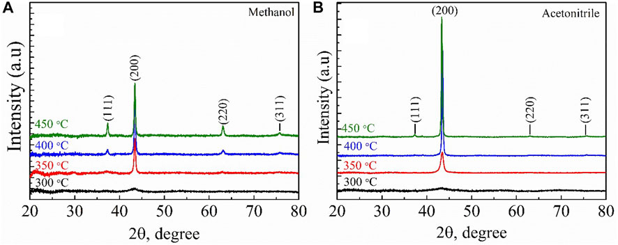
FIGURE 1. X-ray diffraction patterns of NiOx thin films obtained from (A) methanol, and (B) acetonitrile as solvent. The deposition temperatures for NiOx are 300, 350, 400, and 450°C, respectively.
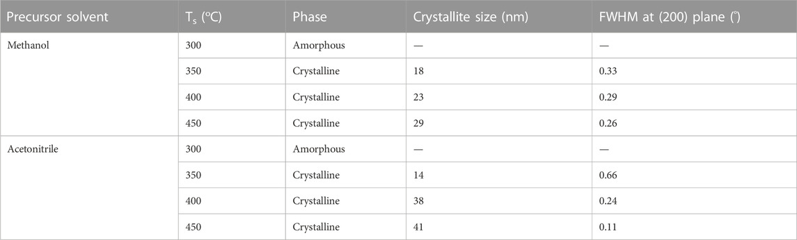
TABLE 1. Influence of deposition temperature and precursor solvent on the crystals structure NiOx thin film, obtained from XRD analysis.
The scanning electron microscope (SEM) images presented in Figure 2 revealed no difference in morphology of the NiOx thin films deposited from methanol- and acetonitrile-based precursors. As depicted in Figure 2A, the NiOx thin film deposited from methanol-based precursor was uniform with fine regular grains which had flat edges, while the films deposited from acetonitrile-based precursor had fine regular grains with rounded edges. However, the mechanisms by which the NiOx grains changed with solvent has not been fully studied at this stage of the work, but it is a known fact that spray from alcohol-based precursors result in much smoother films due to the smaller solution-droplet size (Otto et al., 2011; Krunks et al., 2014).
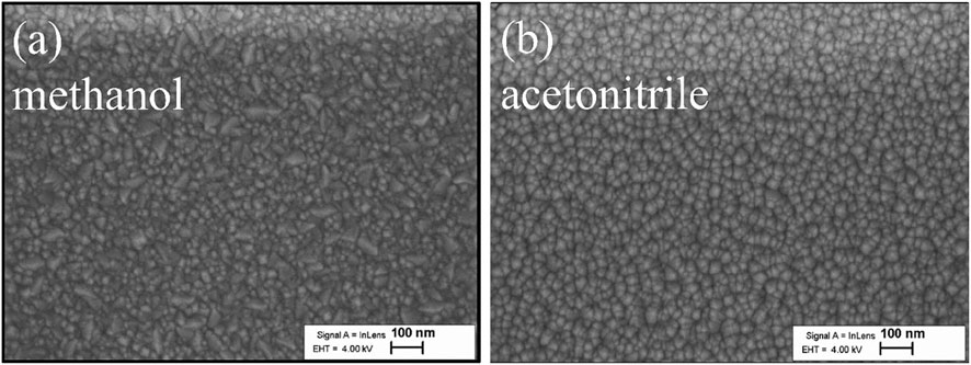
FIGURE 2. Top-down view of SEM images of the deposited NiOx thin film obtained from (A) methanol, and (B) acetonitrile as precursor solvent at Ts = 400°C.
The optical transmittance spectra of NiOx thin film deposited from methanol- and acetonitrile-based precursor is presented in Figure 3A. Both films demonstrated a high optical transmittance along the visible light region and an absorption band edge at around 400 nm, indicating that they could be employed in transparent window applications. Independent of precursor solvent, above 75% transparency was recorded in the deposited NiOx thin films, which surpassed all other reports on NiOx thin film produced using this method (Krunks et al., 2014) (Reguig et al., 2007). The optical bandgap (Eg) values of these thin films were estimated using both the reflectance and transmittance data. According to the transmission spectra, the Eg of NiOx thin films was extrapolated from the Tauc plot (Pankove, 1971). The method was based on the following relation:
where α is the absorption coefficient, hv is the photon energy, A is a constant known as the critical absorption, Eg is the optical energy bandgap (eV), and n is the power coefficient for the respective energy transition. The value of Eg for the deposited NiOx thin films (from methanol- or acetonitrile-based precursor) at different Ts (between 300 and 450°C) were obtained by plotting
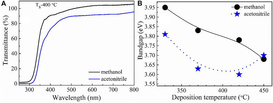
FIGURE 3. (A) Optical transmittance spectra of NiOx films deposited at Ts = 400°C from methanol- and acetonitrile-based precursors, and (B) bandgap variation with deposition temperature for NiOx films deposited at Ts = 400C from methanol- or acetonitrile-based precursors.
To sum-up this part regarding the impact of solvent and growth temperature on the properties of spray-deposited NiOx thin film, it can be inferred that, by changing the solvent, the grain orientation and the NiOx thin film transparency can be tuned. In addition, increasing the growth temperature of NiOx thin film promoted the phase transition from amorphous (in Ts = 300°C) to crystalline (in Ts ≥ 400°C), and these changes were evident in the film’s optical bandgap energy.
3.2 Influence of lithium doping on the morphological, structural, and chemical properties of NiOx thin film
After demonstrating that a uniform and transparent NiOx thin film could be deposited on quartz substrate from a methanol-based precursor by USP, a similar deposition condition could be applied using borosilicate glass, which is suitable for post-deposition annealing (600°C). The condition for depositing Li:NiOx thin film by spray was optimized at Ts = 400°C, and the effect of doping with Li was studied using LiNO3 as the source of Li and Ni (acac)2, due to the fact that relatively uniform and crack-free NiO films were obtained from this precursor. Li:NiOx samples were labelled “y-Li:NiOx” where “y” was an integral number (0, 10, 20, 40, 60) representing the mol% of Li in the spray solution.
Figure 4 shows the surface morphologies of the Li:NiOx thin films with and without 60 mol% of Li in the precursor. Independent of the amount of Li in the solution, the surface morphology of the films was composed of uniform granular grains, and it is important to note that the film was continuous and compact. The film thickness, which was obtained from SEM cross section (image not shown) revealed that the film thickness reduced from 80 nm (0-Li:NiOx) to 55 nm (60-Li:NiOx) with the increase in the amount of Li in the precursor spray solution. The morphology of NiO thin film was similar to that reported by Chan et al. (Chan et al., 2011).
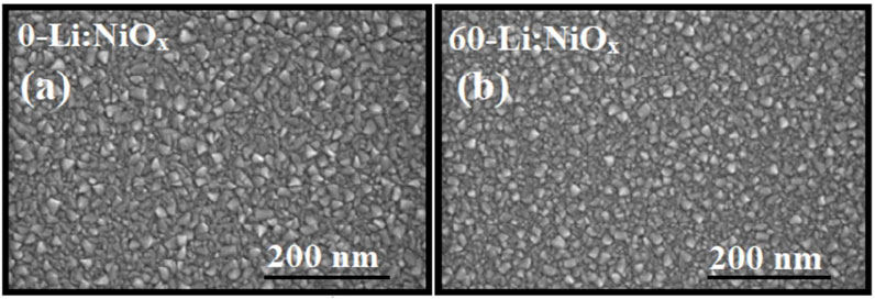
FIGURE 4. SEM images for (A) 0-Li:NiOx and (B) 60-Li:NiOx thin films deposited at 400°C using methanol-based precursor on borosilicate glass substrate.
Figure 5 shows the XRD patterns for Li:NiOx thin films with different doping concentrations of lithium in the precursor solution and the effects of annealing in air and ampoules for 1 h. As seen in Figure 5A, all the as-deposited Li:NiOx thin films were polycrystalline with crystallographic reflection peaks belonging to the cubic NiO phase, and no other phases were suspected. We observed that the introduction of Li into the precursor solution caused an increase in the intensity of the diffraction peak along the (111) plane, and a decrease in the intensity of the (200) diffraction peak. Furthermore, we observed that the addition of Li dopant into the spray solution caused the diffraction peak at the (200) plane to shift from a lower angle of diffraction (2θ = 43.46°) to a higher angle of diffraction (2θ = 43.51°) with the increase in the amount of Li in the solution from 0% to 60%, respectively. The mean crystallite size was calculated to be ca 18.0 nm in the 0-Li:NiOx, ca 6 nm in the 10-Li:NiOx, and later increased to ca 18 nm in the 20-Li:NiOx as-deposited films.
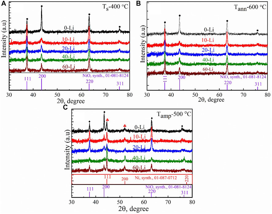
FIGURE 5. X-ray diffraction patterns for (A) (0–60)-Li:NiOx thin films deposited at 400°C from methanol-based precursor, (B) after annealing at 600°C for 1 h in air, and (C) (0–60)-Li:NiOx thin films after annealing in evacuated ampules at 500°C for 1 h. The solid black diamonds represent the crystallographic reflection peaks of cubic NiO, while the solid red clubs represent that of metallic Ni.
On the other hand, Figure 5B shows the XRD pattern of (0–60)-Li:NiOx thin film after annealing in air at 600°C for 1 h. As depicted on the diffractogram, the (0–60)-Li:NiOx films showed a well-defined peak orientation at a similar position to what was previously observed in the as-deposited Li:NiOx. The calculated crystallite sizes and the lattice parameter for both the undoped NiOx and (10–60)-Li:NiOx thin films after annealing at 600°C is presented in Table 2. According to the presented data, it was observed that after annealing at 600°C, the mean crystallite was reduced from 21 nm (in 0-LiNiOx film) to 9 nm (in 10-Li:NiOx film) and later increased to 13 nm (in 40-Li:NiOx film). The XRD pattern did not show any evident changes between the as-deposited and 600°C annealed Li:NiOx thin films, hence the understanding that the doping mechanism at this stage may be very difficult. Furthermore, no Li phases either as Li2O or Li-NiOx alloy was detected in the film. Presumably, because Li was trapped at a defect within the lattice during deposition. In order to understand the Li dopant incorporation, ampoule annealing treatment was done.
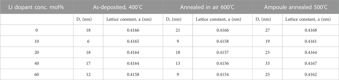
TABLE 2. Changes in the mean crystallite sizes (D) and lattice constant (a) of Li:NiO thin films as a function of Li amount in solution for as-deposited films and after different post-deposition treatment conditions.
Figure 5C represents the XRD result obtained from the (0–60)-Li:NiOx thin film ampoules annealed at 500°C. The diffraction peaks located at 2θ, with values of 37.45, 43.47, 63.11, and 75.69° could be readily indexed as the (111), (200), (220), and (311) crystal planes of the bulk p-NiO respectively, and corresponded to the cubic structure of NiOx, which was in accordance with that of the PDF card No: 01-081-8124. The relative intensity of the peak at the (200) plane decreased, while that of the peak at the (111) plane increased as the amount of Li in the precursor solution was increased. In addition, there occurred two additional peaks at 2θ with values of 44.52° and 51.96° that corresponded to the metallic nickel. The intensity of these peaks increased with the increase in the Li concentration in the precursor solution. It is important to say that the ampoule annealing led to the formation of a mixture of phases and the explanation for this observation is given in the Supplementary Note S1.
To summarize the XRD study, many have reported that Li-doped NiOx favoured crystallization along the (200) plane. This, however, is very subjective, depending on the nature of nickel and lithium sources employed during deposition. For instance, Krunks et al. (Krunks et al., 2014) reported on the growth of Li:NiOx thin film along the (200) plane by spray pyrolysis with LiCl as the dopant source. In our case, the as-deposited Li:NiOx thin film grew along the (111) plane with a reduction in the lattice parameters, which could be associated with Li incorporation within the lattice of the Li:NiOx solid solution formed. Krunks et al. (Krunks et al., 2014) and Tenent et al. (Tenent et al., 2010) also reported no observable deviation between the XRD diffractograms of the lithium-doped and undoped NiOx thin film deposited by spray pyrolysis.
However, as observed in our results, the shift in the 43.47° peak towards a higher angle of diffraction, accompanied by the reduction in the lattice parameters with the increase in the amount of Li in the spray solution, could be explained according to the phenomena which is explained by Bragg’s law (Li et al., 2005) (Lu et al., 2012). This means that, during doping, Li+ impurities have the tendency to substitute Ni2+ and thus reduce the bond length or occupy an interstitial site, resulting in an increase in bond length (Wu and Yang, 2013) (Moulki et al., 2012). A shift in the X-ray diffraction peaks toward a higher 2θ value with the increasing amount of Li in the solution has been reported for solution-processed NiOx thin films (Moulki et al., 2012; Wu and Yang, 2013; Krunks et al., 2014) and for Ni1−xLixO powders (Li et al., 2005; Lu et al., 2012). Maulki et al. (Moulki et al., 2012) explained that when Li+ (0.76 Å) substituted Ni2+ (0.69 Å) in the NiOx film lattice, the formation of a defective Ni3+ (0.56 Å) was induced at an appreciable amount proportional to the amount of the Li incorporated.
According to Deren et al. (Jarzebski, 1973) the conditions for Li atoms to occupy an interstitial position in the Ni-Li-O system are very slight, preferably when the Li amount is approx. 0.2 at.%, which is much lower than our experimental parameters. The annealing process caused an improvement the crystallite growth of Li:NiOx thin film. Although, the isothermal annealing process led to the formation of unexpectedly mixed (NiOx + Ni) phases in the deposited Li:NiOx thin film, it is also worth mentioning that the ampoule annealing process was applied herein for the first time. Sealed evacuated ampoules are a notable technology for homogeneous doping in CdTe (Spalatu et al., 2017) and SnS (Spalatu et al., 2019) chalcogenide photovoltaic materials. Such annealing methods allow the understanding of the mechanism of dopant incorporation into the lattices of thin film material. Based on our results, we claim that during the deposition process Li was incorporated into the NiOx thin film lattice and most probably accumulated at the grain boundaries. Subsequent ampoule annealing at 500°C generated conditions for mass transport through the gas phase, promoting crystallite growth and grain sintering in the NiOx film (as seen on Table 2). The entire process was accompanied by the incorporation and redistribution of Li dopant into the lattice, and it was dictated by the partial pressure of the gas components above the solid NiO phase (the mechanism of the ampoule annealing is described in the Supplementary Note S1).
To ascertain the chemical composition and investigate the changes in the core-level state of the deposited (0, 60)-Li:NiOx thin films, XPS spectra were recorded for each Li 1s, Ni 2p, and O 1s regions. As shown in Figure 6A, the XPS spectra of the Li 1s core level for both as-deposited (0, 60)-Li:NiOx showed no observable peak that corresponded to Li BE, while the (60)-Li:NiOx thin film exhibited a peak at 52.04 ± 0.2 eV BE. Keeping in mind that the relative (to carbon) photoionization cross section of Li was only 0.06 compared to the one of Ni 2p3/2 (13.9) (Trzhaskovskaya et al., 2001), it was no surprise to miss Li 1s signals on the surface of (60)-Li:NiOx. The interesting observation was its detection after isothermal treatment (in ampoules at 500°C) at 52.04 ± 0.2 eV BE, a value attributed in literature to the BE of Li interstitials (Liii) and correlated to the valence state of incomplete oxidation (Lu et al., 2006). One can interpret this by assuming that during the annealing in isothermal conditions, the Li atoms were strongly diffused towards the Li:NiOx surface and detected by XPS.
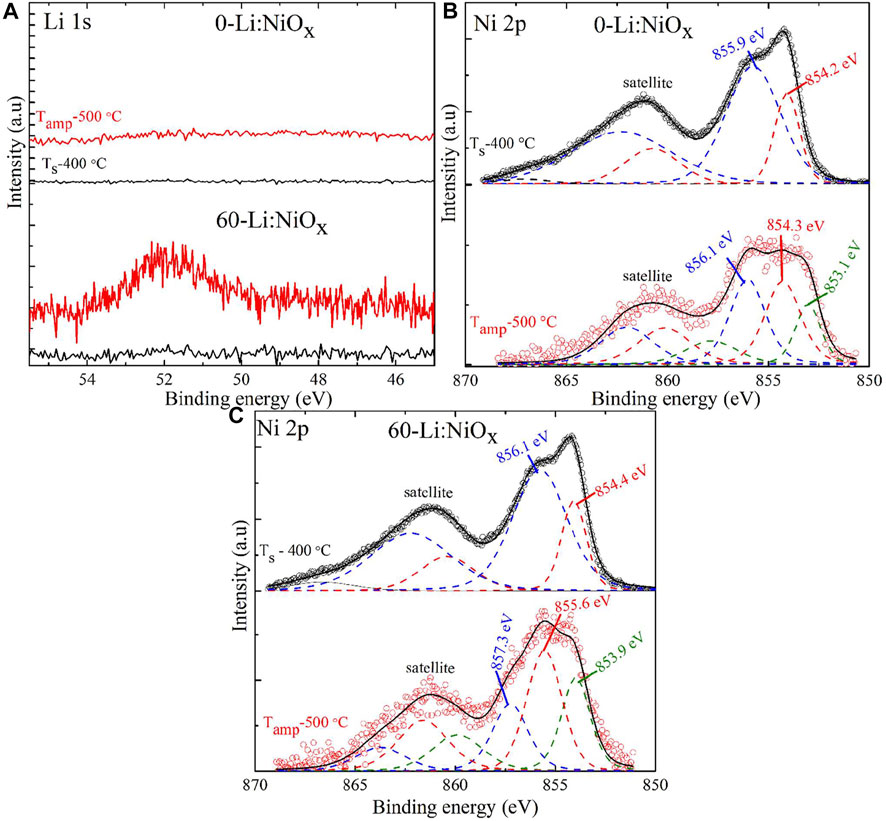
FIGURE 6. X-ray photoelectron core-level spectra for both as-deposited (Ts = 400°C) and ampoule-annealed (Tamp = 500°C) films: (A) Li 1s region for (0, 60)-Li:NiOx, (B) Ni 2p region for the 0-Li:NiOx, and (C) Ni 2p region for the 60-Li:NiOx thin films.
The XPS spectra of Ni 2p core level from the surface of NiOx films (Figure 6B) represented a sum of two envelopes of 5-6 peaks for Ni2+ and Ni3+, and at least one more envelope for nickel hydroxide (Grosvenor et al., 2006). For easy comparison, we have presented here the non-deconvoluted spectra for 0-Li:NiOx and 60-Li:NiOx thin films. As shown in Figures 6B, C, the XPS spectra of Ni 2p peak clearly demonstrated that the NiO (Ni2+ BE at 854.2 ± 0.1 eV) and Ni2O3 (Ni3+ BE at 855.9 ± 0.2 eV) phases coexisted in the 0-Li:NiOx and 60-Li:NiOx films. On comparing the spectra before and after annealing, we observed a shift in the low BE emission in the 0-Li:NiOx films, which was absent in the 60-Li:NiOx films after annealing (Figure 6C). In addition, there was no observable difference between the Ni 2p spectra from undoped and Li-doped NiOx thin films. This indicated that the addition of Li in the precursor solution induced no chemical change in the as-deposited NiOx thin film surface. An illustration of such an observation is presented in the supporting information (Supplementary Figure S2).
In our view, the XPS profile in Figures 6B, C is not asymmetric and there seem to be emissions from other Ni 2p components that are present on the surface of deposited Li:NiOx thin film, thus contributing to the broadness of the peak. To check this assumption, we deconvoluted Ni 2p spectra for the ampoule-annealed NiOx thin films (Supplementary Figure S3) by three main peaks at BE of 853.04 ± 0.2 eV, 854.22 ± 0.2 eV, and 856.06 ± 0.2 eV, and other satellite and shake-up peaks were positioned at 860.44 ± 0.2 eV, and 862.55 ± 0.2 eV (Klein and Hercules, 1986). The O 1s core-level spectral for as-deposited Li:NiOx thin film at different amount of Li in the spray precursor solution are given in the supporting information (Supplementary Figure S4). Based on literature records, the peak at low BE 853.04 ± 0.2 eV could be attributed to Ni-atoms in the zero state (Ni0), the peak at 860.44 ± 0.2 eV—to its satellite peak, whereas the peaks at 854.29 ± 0.2 eV and 856.04 ± 0.2 eV BE were attributed to Ni2+, and Ni3+, respectively (Lei et al., 2014) (Soo Kim and Lee, 2012). This result supports the current observation of metallic (Ni0) by the XRD analysis after the ampoule-annealing process, and the explanation is given in the Supplementary Material.
3.3 Electrical properties of Li:NiOx thin film
The electrical properties of the spray-deposited (0–60)-Li:NiOx thin film were measured using the van der Pauw method at room temperature, and the results are presented in Table 3. According to the electrical results of the as-deposited (0–60)-Li:NiOx thin films as a function of Li concentration in the precursor solution, all the deposited Li:NiOx films exhibited p-type electrical conductivity as determined by hot probe technique and verified by the sign of the Hall coefficient. The resistivity of 0-Li:NiOx thin film was 2.2 × 10⁴ Ωcm; increasing the Li amount in the precursor solution yielded a resistivity value of 3.6 × 10² Ω-cm for the 60-Li:NiOx films. This was because the amount of Li atoms available to replace the sites of Ni atoms increased, and the carrier (hole) concentration increased from 3.0 × 10¹³ to 5.0 × 1015 cm−3. The carrier mobility of the Li:NiOx thin films decreased from 6.0 cm2/(Vs.) to 1.5 cm2/(Vs.) as the amount of Li in the precursor solution was increased from 0 to 60 mol%. In Li:NiOx thin films, the Li atom, which was the dopant material, can act as scattering centres; as the amount of Li was increased, the carriers were trapped within the film matrix, thus resulting in a decrease in carrier mobility. Based on the electrical properties of the as-deposited samples (0-60)-Li:NiOx, it could be inferred that the sprayed-deposited Li:NiOx thin film may not be sufficiently conductive to yield higher carrier concentrations (ρ ≥ 10–4 Ω cm), indicating no significant density of electrically active defects, i.e., Ni vacancies (VNi). Several authors have reported a lower resistive NiO thin film in the order of 300 Ωcm by spray pyrolysis and other solution-based methods when NiNO3 was used as Ni source (Moulki et al., 2012; Wu and Yang, 2013; Krunks et al., 2014).
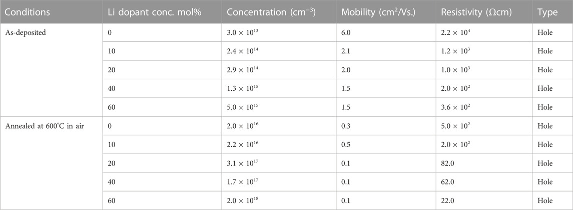
TABLE 3. Carrier concentration, mobility, and resistivity of the as-deposited at 400°C and 600°C annealed Li:NiOx thin films as a function of Li amount in the precursor solution.
To further improve the electrical properties of the deposited Li:NiOx thin films, post-deposition thermal annealing in air at 600°C was carried out. Sequential measurements were made to extract reliable carrier concentration (p) and mobility (μ) data during the Hall effect measurement. The result obtained from the (60)-Li:NiOx thin film after annealing in air at 600°C showed a decrease in resistivity (∼22 Ωcm), a decrease in mobility (∼0.1 cm2/Vs.), and a two orders of magnitude increase in carrier concentration (∼2.0 × 1018 cm−3) relative to the as-deposited Li:NiOx films. To explain the impact of Li doping concentration on the enhanced carrier density in Li:NiOx films, the changes in the structural properties of the films should be also considered. Although grain size and grain boundaries have a major impact on the electrical parameters, no evident changes in the morphology of the Li:NiOx films were observed with the increase of Li dopant concentration. Moreover, according to XRD analysis, for both as-deposited and 600°C air-annealed Li:NiOx thin films, the crystallite size decreased with the increase of Li dopant concentration from 10 to 60 mol% (Table 2). Thus, these results indicated that the resulting hole concentration in Li:NiOx was greatly impacted by the concentration of intrinsic point defects rather than by the changes in the crystallite size (and consequently grain size) of the films. Considering the vacancy-type mechanism as a predominant disorder in the NiO films, the defect formation within the NiOx lattice with incorporation of Li led to the generation of holes. With the addition of Li, more Li+ ions substituted Ni2+ sites in the original crystal structure and created more holes into the NiOx lattice. The detailed mechanism of the formation of Schottky defects (considering the equilibrium constant in the NiOx lattice) is described in the Supplementary Note S1. Although the Li dopant enhanced the hole density in Li:NiOx films, the decrease in the mobility (Table 3) was an indication that the Li dopant may imply scattering phenomena via ionized impurity. On the other hand, there was a strong hindrance in the deposited Li:NiOx films, which was consequently due to the presence of grain boundaries, electrically active defects, and/or impurities playing an influential role in determining the transport properties of polycrystalline films (Zhang et al., 2018).
It is worth mentioning that several authors have reported the resistivity values of the NiOx and doped NiOx films in the range of 10−1 to 10−3 Ωcm after post-deposition annealing in the temperature range of 400–600°C (Tyagi et al., 2013; Menchini et al., 2013; Jlassi et al., 2014; Ivanova et al., 2022; Wu and Yang, 2013). The specific values largely depended on the employed deposition methods and the annealing ambient conditions (Jlassi et al., 2014; Pan et al., 2019; Ivanova et al., 2022). A common peculiarity for most of the previous studies is that the as-grown NiOx films were always amorphous and/or exhibited very low crystallinity, independent of the method employed for the film synthesis. This implied that a second step of post-deposition annealing was required and usually the treatment should be performed at temperatures between 500 and 600°C. The results in this work show that by changing the solvent, the grain orientation and the NiOx thin film transparency can be tuned and, importantly, by selection a proper solvent for the USP precursor, the temperature at which phases transition from amorphous to crystalline can be significantly lowered. These findings provide complementary knowledge to that already existing about wet-chemical methods, showing that Li:NiO films fabricated by ultrasonic spray, which is a large-area wet-chemical method, within the precursor system of Ni-acetylacetonate- LiNO3- acetonitrile allowed the fabrication of crystalline NiOx films at 400°C. It was demonstrated that the incorporation of Li in NiOx decreased the mean crystallite size of the films by a factor of two compared to those undoped. Furthermore, p-type conductivity, resistivity, and carrier concentration could be tuned by controlling the amount of Li in the precursor solution. The 600°C annealing of NiOx films with 10 mol% Li in the precursor solution was identified as the optimal temperature to result in films with resistivity of 2.0 × 10² Ωcm and a carrier concentration of 2.2 × 1016 cm−3. Thus, ultrasonic spray pyrolysis is a reliable method, allowing an alternative wet-chemical method for the large-scale production of the p-type NiO films fabrication, and the suitability of these films for application due to the hole transport layers in inverted solar cells.
4 Conclusion
We have demonstrated the deposition of NiOx and Li:NiOx thin films by ultrasonic spray pyrolysis method with a precursor prepared by combinative mixing of nickel acetylacetonate salt in either methanol or acetonitrile solvents. The choice of solvent and growth temperature was found to influence the morphological, structural, optical, chemical, and electrical properties of the deposited NiOx thin films. The deposited NiOx thin films were uniform and well compact. The optical studies gave evidence that the bandgap of USP-deposited NiOx thin film at 400°C could be tuned from 3.59 eV to 3.78 eV when changing the solvent of the precursor from acetonitrile to methanol. According to the XRD analysis, the deposited NiOx films (from both methanol- and acetonitrile-based precursors) were polycrystalline with a mean crystallite size ranging from 18 to 30 nm (methanol based) and from 14 to 41 nm (acetonitrile-based) when the deposition temperature was varied from 350 to 450°C. To improve the electrical properties of spray deposited NiOx, the doping of NiOx films with monovalent Li+ was employed. The deposited Li:NiOx thin films exhibited uniform morphology and a p-type conductivity. The incorporation of Li in NiOx thin film was confirmed by both XRD and XPS analyses. Li+ doping in form of Li-NiOx alloy solution reduced the electrical resistivity of the as-deposited thin film, from 104 to 102 Ω cm, and increased the carrier concentration by two orders of magnitude as the lithium concentration in the precursor solution increased, from 0 to 60 mol%. An additional annealing step at 600°C in air resulted in a further three orders of magnitude enhancement in hole concentration. Based on these results, the mechanism of Li incorporation with the formation of point defects was proposed. This work provides new insight into the fundamental understanding of the doping mechanism in NiOx, and brings technical advances in the fabrication of p-type conductivity in Li-doped NiOx, a functional hole transport material for solar cells.
Data availability statement
The original contributions presented in the study are included in the article/Supplementary Material, further inquiries can be directed to the corresponding authors.
Author contributions
AO: conceptualization, methodology, validation, formal analysis, investigation, writing—original draft, visualization. NS: conceptualization, investigation, formal analysis, writing—review and editing, resources. NM: XPS data acquisition, writing—review and editing. AK: validation of XPS data. AM: resources, validation. MK: conceptualization, resources, writing—review and editing, supervision, project administration, funding acquisition. IA: conceptualization, resources, writing—review and editing, supervision, project administration, funding acquisition.
Funding
All of the sources of funding for the work described in this publication are acknowledged below: Estonian Research Council project PRG627 “Antimony chalcogenide thin films for next-generation semi-transparent solar cells applicable in electricity producing windows.” Estonian Research Council project PSG689 “Bismuth Chalcogenide Thin-Film Disruptive Green Solar Technology for Next-Generation Photovoltaics.” Estonian Centre of Excellence project TK141 (TAR16016EK) “Advanced materials and high-technology devices for energy recuperation systems.” The European Union’s H2020 Programme under the ERA Chair project 5GSOLAR grant agreement No. 952509.
Acknowledgments
The authors also thank Valdek Mikli and Olga Volobujeva from the Laboratory of Optoelectronic Materials Physics at Tallinn University of Technology for recording the SEM images.
Conflict of interest
The authors declare that the research was conducted in the absence of any commercial or financial relationships that could be construed as a potential conflict of interest.
Publisher’s note
All claims expressed in this article are solely those of the authors and do not necessarily represent those of their affiliated organizations, or those of the publisher, the editors and the reviewers. Any product that may be evaluated in this article, or claim that may be made by its manufacturer, is not guaranteed or endorsed by the publisher.
Supplementary material
The Supplementary Material for this article can be found online at: https://www.frontiersin.org/articles/10.3389/fmats.2023.1060420/full#supplementary-material
References
Alver, U., Yaykash¸, H., Kerli, S., and Tanrıverdi, A. (2013). Synthesis and characterization of boron-doped NiO thin films produced by spray pyrolysis. Int. J. Min. Metall. 20 (11), 1097–1101. doi:10.1007/s12613-013-0839-8
Barquinha, P., Martins, R., Pereira, L., and Fortunato, E. (2012). Transparent oxide electronics: From material to devices. United Kingdom: John Wiley and Sons.
Caruge, J. M., Halpert, J. E., Bulovic, V., and Bawendi, M. G. (2006). NiO as an inorganic hole-transporting layer in quantum-dot light-emitting devices. Nano Lett. 6, 2991–2994. doi:10.1021/nl0623208
Chan, X. H., Jennings, J. R., Hossain, M. A., Yu, K. K. Z., and Wang, Q. (2011). Characteristics of p-NiO thin films prepared by spray pyrolysis and their application in CdS-sensitized photocathodes. Electrochem. Soc. 158, H733–H740. doi:10.1149/1.3590742
Chen, X., Zhao, L., and Niu, Q. I. (2012). Electrical and optical properties of p-type Li,Cu-codoped NiO thin films. J. Electron. Mater. 41 (12), 3382–3386. doi:10.1007/s11664-012-2213-4
Chen, Z., Dedova, T., Oja-Acik, I., Danilson, M., and Krunks, M. (2021). Nickel oxide films by chemical spray: Effect of deposition temperature and solvent type on structural, optical, and surface properties. Appl. Surf. Sci. 548, 149118. doi:10.1016/j.apsusc.2021.149118
Chen, Z., Dedova, T., Spalatu, N., Maticiuc, N., Rusu, M., Katerski, A., et al. (2022). ZnO/NiO heterostructures with enhanced photocatalytic activity obtained by ultrasonic spraying of a NiO shell onto ZnO nanorods. Colloids Surfaces A Physicochem. Eng. Aspects 648, 129366. doi:10.1016/j.colsurfa.2022.129366
Desai, J. D., Min, S.-K., Jung, K.-D., and Joo, O.-S. (2006). Spray pyrolytic synthesis of large area NiO x thin films from aqueous nickel acetate solutions. Appl. Surf. Sci. 253, 1781–1786. doi:10.1016/j.apsusc.2006.03.009
Eensalu, J. S., Katerski, A., Kärber, E., Weinhardt, L., Blum, M., Heske, C., et al. (2019). Semitransparent Sb2S3 thin film solar cells by ultrasonic spray pyrolysis for use in solar windows. Beilstein J. Nanotechnol. 10, 2396–2409. doi:10.3762/bjnano.10.230
Eensalu, J. S., TõnsuaaduOja Acik, K. I., and Krunks, M. (2022). Sb2S3 thin films by ultrasonic spray pyrolysis of antimony ethyl xanthate. Mater. Sci. Semicond. Process. 137, 106209. doi:10.1016/j.mssp.2021.106209
Gomaa, M. M., Yazdi, G. R., Schmidt, S., Boshta, M., Khranovskyy, V., Eriksson, F., et al. (2017). Effect of precursor solutions on the structural and optical properties of sprayed NiO thin films. Mat. Sci. Semicond. process. 64, 32–38. doi:10.1016/j.mssp.2017.03.009
Goodenough, J. B., Wickham, D. G., and Croft, W. J. (1958). Some magnetic and crystallographic properties of the system Li+xNi++1−2xni+++xO. J. Phys. Chem. Solids 5, 107–116. doi:10.1016/0022-3697(58)90136-7
Grosvenor, A. P., Biesinger, M. C., Smart, R. C., and McIntyrea, N. S. (2006). New interpretations of XPS spectra of nickel metal and oxides. Surf. Sci. 600 (9), 1771–1779. doi:10.1016/j.susc.2006.01.041
Guo, W., Hui, K. N., and Hui, K. S. (2013). High conductivity nickel oxide thin films by a facile sol–gel method. Mat. Lett. 92, 291–295. doi:10.1016/j.matlet.2012.10.109
International Centre for Diffraction Data (ICDD) (2008). Powder Diffraction File (PDF). PDF-2 Release 2008.
Irwin, M. D., Buchholz, D. B., Hains, A. W., and Marks, T. J. (2008). p -Type semiconducting nickel oxide as an efficiency-enhancing anode interfacial layer in polymer bulk-heterojunction solar cells. Proc. Natl. Acad. Sci. U. S. A. 105, 2783–2787. doi:10.1073/pnas.0711990105
Ivanova, T., Harizanova, A., Shipochka, M., and Vitanov, P. (2022). Nickel oxide films deposited by sol-gel method: Effect of annealing temperature on structural, optical, and electrical properties. Materials 15 (5), 1742. doi:10.3390/ma15051742
Jarzebski, Z. M. (1973). Metal oxide semiconductor crystals - defects. Oxford: Pergamon Press, 184–186.
Jeng, J. Y., Chen, K. C., Chiang, T. Y., Lin, P. Y., Tsai, T. D., Chang, Y. C., et al. (2014). Nickel oxide electrode interlayer in CH3NH3PbI3Perovskite/PCBM planar-heterojunction hybrid solar cells. Adv. Mat. 26, 4107–4113. doi:10.1002/adma.201306217
Jlassi, M., Sta, I., Hajji, M., and Ezzaouia, H. (2014). Optical and electrical properties of nickel oxide thin films synthesized by sol–gel spin coating. Mater. Sci. Semicond. Process. 21 (1), 7–13. doi:10.1016/j.mssp.2014.01.018
Joseph, D. P., Saravanan, M., Muthuraaman, B., Renugambal, P., Sambasivam, S., Philip Raja, S., et al. (2008). Spray deposition and characterization of nanostructured Li doped NiO thin films for application in dye-sensitized solar cells. Nanotechnology 19, 485707. doi:10.1088/0957-4484/19/48/485707
Jošt, M., Bertram, T., Koushik, D., Marquez, J. A., Verheijen, M. A., Heinemann, M. D., et al. (2019). 21.6%-Efficient monolithic perovskite/Cu(in,Ga)Se2 tandem solar cells with thin conformal hole transport layers for integration on rough bottom cell surfaces. ACS Energy Lett. 4, 583–590. doi:10.1021/acsenergylett.9b00135
Juneja, N., Mandati, S., Katerski, A., Spalatu, N., Daskeviciute-Geguziene, S., Vembris, A., et al. (2022). Sb 2 S 3 solar cells with a cost-effective and dopant-free fluorene-based enamine as a hole transport material. Sustain. Energy and Fuels 6 (13), 3220–3229. doi:10.1039/d2se00356b
Juybari, H. A., Bagheri-Mohagheghi, M.-M., and Shokooh-Saremi, M. (2011). Nickel-lithium oxide alloy transparent conducting films deposited by spray pyrolysis technique. J. Alloys Compd. 509, 2770–2775. doi:10.1016/j.jallcom.2010.11.075
Kamal, H., Elmaghraby, E. K., Ali, S. A., and Abdel-Hady, K. (2004). Characterization of nickel oxide films deposited at different substrate temperatures using spray pyrolysis. J. Cryst. Growth 262, 424–434. doi:10.1016/j.jcrysgro.2003.10.090
Klein, J. C., and Hercules, D. M. (1986). Surface characterization of model Urushibara catalysts. J. Catal. 82 (2), 424–441. doi:10.1016/0021-9517(83)90209-9
Koltsov, M., Krautmann, R., Katerski, A., Maticiuc, N., Krunks, M., Oja Acik, I., et al. (2022). A post-deposition annealing approach for organic residue control in TiO2 and its impact on Sb2Se3/TiO2 device performance. Faraday Discuss. 239, 273. doi:10.1039/d2fd00064d
Krautmann, R., Spalatu, N., Josepson, R., Nedzinskas, R., Kondrotas, R., Gržibovskis, R., et al. (2023). Low processing temperatures explored in Sb2S3 solar cells by close-spaced sublimation and analysis of bulk and interface related defects. Sol. Energy Mater. Sol. Cells 251, 112139. doi:10.1016/j.solmat.2022.112139
Krunks, M., Soon, J., Unt, T., Mere, A., and Mikli, V. (2014). Deposition of p-type NiO films by chemical spray pyrolysis. Vacuum 107, 242–246. doi:10.1016/j.vacuum.2014.02.013
Lauermann, I., and Steigert, A. (2016). CISSY: A station for preparation and surface/interface analysis of thin film materials and devices. J. Large Scale Res. Facil. JLSRF 2, A67. doi:10.17815/jlsrf-2-84
Lei, Y., Li, J., Wang, Y., Gu, L., Chang, Y., Yuan, H., et al. (2014). Rapid microwave-assisted green synthesis of 3D hierarchical flower-shaped NiCo2O4 microsphere for high-performance supercapacitor. ACS Appl. Mat. Interfaces 6, 1773–1780. doi:10.1021/am404765y
Li, Z., Wang, C., Ma, X., Yuan, L., and Sun, J. (2005). Synthesis, structures and electrochemical properties of Li xNi1-xO. Mater. Chem. Phys. 91 (1), 36–39. doi:10.1016/j.matchemphys.2004.10.043
Lu, J. G., Zhang, Y. Z., Ye, Z. Z., Zeng, Y. J., He, H. P., Zhu, L. P., et al. (2006). Control of p- and n-type conductivities in Li-doped ZnO thin films. Appl. Phys. Lett. 89, 112113. doi:10.1063/1.2354034
Lu, Y., Hao, L., Yoshida, H., and Hirohashi, M. (2012). Reaction behaviour of Ni 1-x M x O's (M = Li, Na) formation and its thermoelectric properties. J. Mater. Sci. Mater. Electron. 23 (1), 315–319. doi:10.1007/s10854-011-0411-0
Menchini, F., Grilli, M., Dikonimos, T., Mittiga, A., Serenelli, L., Salza, E., et al. (2013). Application of NiOx thin films as p-type emitter layer in heterojunction solar cells. Wiley Online Libr. 13 (10-12), 1006–1010. doi:10.1002/pssc.201600121
Moulki, H., Park, D. H., Min, B.-K., Kwon H, H., Hwang, S. -J., Choy, J. -H., et al. (2012). Improved electrochromic performances of NiO based thin films by lithium addition: From single layers to devices. Electrochimica Acta 74, 46–52. doi:10.1016/j.electacta.2012.03.123
Napari, M., Huq, T. N., Hoye, R. L. Z., and MacManus-Driscoll, J. L. (2020). Nickel oxide thin films grown by chemical deposition techniques: Potential and challenges in next-generation rigid and flexible device applications. InfoMat 3, 536–576. doi:10.1002/inf2.12146
Ohta, H., Hirano, M, and Hosono, H. (2003a). Fabrication and photoresponse of a pn-heterojunction diode composed of transparent oxide semiconductors, p-NiO and n-ZnO. Appl. Phys. Lett. 83, 1029–1031. doi:10.1063/1.1598624
Ohta, H., Kamiya, M., Kamaiya, T., Hirano, M., and Hosono, H. (2003b). UV-detector based on pn-heterojunction diode composed of transparent oxide semiconductors, p-NiO/n-ZnO. Thin Solid Films 317, 317–321. doi:10.1016/s0040-6090(03)01178-7
Oluwabi, A. T., Katerski, A., Carlos, E., Branquinho, R., Mere, A., Krunks, M., et al. (2020). Application of ultrasonic sprayed zirconium oxide dielectric in zinc tin oxide-based thin film transistor. J. Mat. Chem. C 8, 3730–3739. doi:10.1039/c9tc05127a
Otto, K., Katerski, A., Volobujeva, O., Mere, A., and Krunks, M. (2011). Indium sulfide thin films deposited by chemical spray of aqueous and alcoholic solutions. Energy Procedia 3, 63–69. doi:10.1016/j.egypro.2011.01.011
Pan, Y., Li, L., Yu, S., Zheng, H., and Peng, W. (2019). The annealing temperature and films thickness effect on the surface morphology, preferential orientation and dielectric property of NiO films. Appl. Surf. Sci. 493, 396–403. doi:10.1016/j.apsusc.2019.06.223
Pankove, J. I. (1971). Optical process in semiconductors. Eaglewood Cliffs, N. J: Prentice-Hall, 422.
PanLingxia, Y. L., ShihuiHaoran, Y. Z., and Wei, P. (2019). The annealing temperature and films thickness effect on the surface morphology, preferential orientation and dielectric property of NiO films. Appl. Surf. Sci. 493, 396–403. doi:10.1016/j.apsusc.2019.06.223
Reguig, B. A., Khelil, A., Cattin, L., Morsli, M., and Berne`de, J. C. (2007). Properties of NiO thin films deposited by intermittent spray pyrolysis process. Appl. Surf. Sci. 253, 4330–4334. doi:10.1016/j.apsusc.2006.09.046
Sato, H., Minami, T., Takata, S., and Yamada, T. (1993). Transparent conducting p-type NiO thin films prepared by magnetron sputtering. Thin Solid Films 27, 27–31. doi:10.1016/0040-6090(93)90636-4
Soo Kim, D., and Lee, C. (2012). Nickel vacancy behavior in the electrical conductance of nonstoichiometric nickel oxide film. J. Appl. Phys. 112, 034504. doi:10.1063/1.4742993
Spalatu, N., Hiie, J., Kaupmees, R., Volobujeva, O., Krustok, J., Oja Acik, I., et al. (2019). Postdeposition processing of SnS thin films and solar cells: Prospective strategy to obtain large, sintered, and doped SnS grains by recrystallization in the presence of a metal halide flux. ACS Appl. Mat. Interfaces 11, 17539–17554. doi:10.1021/acsami.9b03213
Spalatu, N., Krunks, M., and Hiie, J. (2017). Structural and optoelectronic properties of CdCl2 activated CdTe thin films modified by multiple thermal annealing. Thin Solid Films 633, 106–111. doi:10.1016/j.tsf.2016.09.042
Tenent, R. C., Gillaspie, D. T., Miedaner, A., Parilla, P. A., Curtis, C. J., and Dillon, A. C. (2010). Fast-switching electrochromic Li[sup +]-Doped NiO films by ultrasonic spray deposition. J. Electrochem Soc. 157, H318–H322. doi:10.1149/1.3279992
Trzhaskovskaya, M. B., Nefedov, V. I., and Yarzhemsky, V. G. (2001). Photoelectron angular distribution parameters for elements Z=1 to Z=54 in the photoelectron energy range 100–5000 ev. Atomic Data Nucl. Tables 77, 97–159. doi:10.1006/adnd.2000.0849
Tyagi, M., Tomar, M., and Gupta, V. (2013). Postdeposition annealing of NiOx thin films: A transition from n-type to p-type conductivity for short wave length optoelectronic devices. J. Mater. Res. 28 (5), 723–732. doi:10.1557/jmr.2012.443
W Han, S., H Kim, I., H Kim, D., Park, K. J., Park, E. J., Jeong, M. G., et al. (2016). Temperature regulated chemical vapor deposition for incorporating NiO nanoparticles into mesoporous media. Appl. Surf. Sci. 385, 597–604. doi:10.1016/j.apsusc.2016.05.160
Williams, P. A., Jones, A. C., Bickley, J. F., Steiner, A., Davies, H. O., Leedham, T. J., et al. (2001). Synthesis and crystal structures of dimethylaminoethanol adducts of Ni(II) acetate and Ni(II) acetylacetonate. Precursors for the sol–gel deposition of electrochromic nickel oxide thin films. J. Mat. Chem. 11, 2329–2334. doi:10.1039/b103288g
Wu, C-C., and Yang, C-F. (2013). Fabricate heterojunction diode by using the modified spray pyrolysis method to deposit Nickel−Lithium oxide on indium tin oxide substrate. ACS Appl. Mat. Interfaces 5, 4996–5001. doi:10.1021/am400763m
Xia, X., Tu, J., Zhang, J., Wang, X., Zhang, W., and Huang, H. (2008). Electrochromic properties of porous NiO thin films prepared by a chemical bath deposition. Sol. Energy Mater Sol. Cells 92 (6), 628–633. doi:10.1016/j.solmat.2008.01.009
Yang, C. F., and Wu, C. C. (2015). Effect of annealing temperature on the characteristics of the modified spray deposited Li-doped NiO films and their applications in transparent heterojunction diode. Sol. Energy Mater. Sol. Cells 132, 492–498. doi:10.1016/j.solmat.2014.09.017
Yu, S., Liu, X., Yang, P., Wu, C., and Li, L. (2022). Flexible transparent Ag nanowire/UV-curable resin heaters with ultra-flexibility, high transparency, quick thermal response, and mechanical reliability. J. Alloys Compd. 908, 164690. doi:10.1016/j.jallcom.2022.164690
Yu, S., Liu, X., Yang, P., Zhao, L., Dong, H., Wu, C., et al. (2022). Highly stable silver nanowire networks with tin oxide shells for freestanding transparent conductive nanomembranes through all-solution processes. Chem. Eng. J. 446, 137481. doi:10.1016/j.cej.2022.137481
Yu, S., Zhang, W., Li, L., Dong, H., Xu, D., and Jin, Y. (2014). Structural, electrical, photoluminescence and optical properties of n–type conducting, phosphorus-doped ZnO thin films prepared by pulsed laser deposition. Appl. Surf. Sci. 298, 44–49. doi:10.1016/j.apsusc.2014.01.037
Zhang, J. Y., Li, W. W., Hoye, R. L. Z., MacManus-Driscoll, J. L., Budde, M., Bierwagen, O., et al. (2018). Electronic and transport properties of Li-doped NiO epitaxial thin films. RSC Mat. Chem. C 6 (9), 2275–2282. doi:10.1039/c7tc05331b
Keywords: NiO, Li doped NiOx, thin film, acetylacetonate, ultrasonic spray pyrolysis, postdeposition treatment
Citation: Oluwabi AT, Spalatu N, Maticiuc N, Katerski A, Mere A, Krunks M and Acik IO (2023) Combinative solution processing and Li doping approach to develop p-type NiO thin films with enchanced electrical properties. Front. Mater. 10:1060420. doi: 10.3389/fmats.2023.1060420
Received: 03 October 2022; Accepted: 11 January 2023;
Published: 02 February 2023.
Edited by:
Katherine Hooper, Swansea University, United KingdomCopyright © 2023 Oluwabi, Spalatu, Maticiuc, Katerski, Mere, Krunks and Acik. This is an open-access article distributed under the terms of the Creative Commons Attribution License (CC BY). The use, distribution or reproduction in other forums is permitted, provided the original author(s) and the copyright owner(s) are credited and that the original publication in this journal is cited, in accordance with accepted academic practice. No use, distribution or reproduction is permitted which does not comply with these terms.
*Correspondence: Abayomi T. Oluwabi, YWJheW9taW9sdXdhYmlAZ21haWwuY29t; Nicolae Spalatu, bmljb2xhZS5zcGFsYXR1QHRhbHRlY2guZWU=