 Jiajiu Ye1,2*
 Stéphanie Pouget
 Dmitry Aldakov
 Yueli Liu
 Peter Reiss
- 1CEA, CNRS, INP, IRIG/SyMMES, University Grenoble-Alpes, Grenoble, France
- 2Hefei Institute of Physical Science, CAS, Hefei, China
- 3CEA, IRIG/MEM, SGX, University Grenoble-Alpes, Grenoble, France
- 4State Key Laboratory of Silicate Materials for Architectures, School of Materials Science and Engineering, Wuhan University of Technology, Wuhan, China
Tin (IV) oxide is a highly promising electron transport layer (ETL) for lead halide perovskite solar cells due to its high conductivity, transparency, wide band gap, and the possibility of low-temperature processing. Nonetheless, charge carrier recombination processes at the SnO2/perovskite interface diminish the device performance. Here, we demonstrate that SnO2 doping with guanidine hydrochloride (G-SnO2) leads to efficient surface passivation and a larger band offset between the ETL and the perovskite layer, resulting in reduced voltage losses and faster electron transfer. Moreover, G-SnO2 facilitates the growth of highly crystalline perovskite layers. Consequently, a power conversion efficiency of up to 23.48% and a high open-circuit voltage of 1.18 V are obtained in solar cells incorporating the G-SnO2 ETL. These devices also exhibited negligible hysteresis and maintained more than 96% of their initial power conversion efficiency after 1,250 h exposure to the air without encapsulation.
1 Introduction
The electron transport layer (ETL) is one essential part of perovskite solar cells (PSCs), assuring electron extraction from the perovskite layer and blocking holes to avoid undesired recombination processes. (Ke et al., 2015; Anaraki et al., 2016; Jiang et al., 2016). An ideal ETL should possess high electron mobility, favorable energy level alignment with the active layer, and good processability for the preparation of high-quality films. Amongst the N-type semiconductor used for the fabrication of ETLs, WOx, NbOx, CeOx, and BaSnO3 can be found along with the more widely used materials TiO2, ZnO, and SnO2. (Murugadoss et al., 2016; Lee et al., 2017; Zhu et al., 2017). In this group, SnO2 is a highly promising candidate owing to (i) its high electron mobility (over 420 cm2/V.s), favoring efficient transport; (ii) its wide energy band gap, giving rise to fewer losses due to parasitic light absorption; (iii) its low annealing temperature, normally less than 150 °C, which enables the fabrication of solar cells at a lower cost and on various types of substrates including flexible ones. (Tu et al., 2019; Wang et al., 2020a; Xiong et al., 2022).
To overcome limitations originating from undesired recombination processes at the SnO2/perovskite interface, which are related to sub-optimal energy level alignment and interfacial defect states, (Sutanto et al., 2021; Liu et al., 2022; Odunmbaku et al., 2022), surface modification of the ETL is a commonly used approach. Various kinds of passivating agents have been reported, for example, inorganic salts, long-chain polymers, and small organic molecules. (Zhao et al., 2018; Jiang et al., 2019; Fu et al., 2020). As an example, Huang and coworkers demonstrated that passivation of the SnO2 ETL with potassium ions (from KOH) eliminated hysteresis effects and influenced the growth of the perovskite grains, resulting in enhanced efficiency and stability. (Bu et al., 2018). Potassium chloride (KCl) has also been used for passivating SnO2 thin films. (Jalebi et al., 2018; Wang et al., 2018; Qin et al., 2019). More recently, Yu et al. reported the use of guanidinium chloride for the treatment of the SnO2 ETL to eliminate detrimental O2− species formed at its surface during thermal annealing, which led to an improvement of the power conversion efficiency (PCE) of the obtained perovskite solar cells from 15.33% to 18.46%. (Yu et al., 2020).
Compared with these post-deposition surface treatment procedures of the annealed ETL layer, in situ bulk doping of the ETL via the addition of appropriate molecular species during its preparation is an alternative approach to fine-tune its properties. (Jung et al., 2013; Ren et al., 2017; Huang et al., 2018). In particular, it can give access to increased conductivity of the ETL due to electrical doping, which is often accompanied by the positive side effect of lower annealing temperatures required for the ETL preparation. Moreover, the judicious choice of additives can lead to better control of the band alignment at the ETL/perovskite interface favoring efficient charge transfer. As an example, Li and coworkers adopted electron-donating triphenylphosphine oxide (TPPO) as a dopant of the SnO2 layer, which enhanced its conductivity and decreased the energy barrier at perovskite/SnO2 interface from 0.55 to 0.39 eV, resulting in a PCE of 20.69%. (Deng et al., 2020). In another example, Zheng and coworkers applied KF-doped SnO2 to improve the performance of all-inorganic CsPbI2Br solar cells showing an open-circuit voltage (Voc) of 1.31 V (Zhang et al., 2021). In our previous work, we investigated ammonium chloride as a dopant for SnO2, employing a double-layer ETL with different doping levels. This approach led to a significant improvement in the performance of planar PSCs due to a more favorable energy level alignment at the ETL/perovskite interface, resulting in a Voc of 1.21 V and a PCE of 21.75% (pristine ETL: 1.14 V, 18.54%). (Ye et al., 2021).
Based on these results, we explore here guanidine hydrochloride (H2N)2C = NH2+Cl−, also known as guanidinium chloride (Gua-Cl), as a bulk dopant for the SnO2 ETL. Gua has been previously used mainly for improving the stability of PSCs by incorporating this large cation into the perovskite layer. (Ishibashi et al., 2017; Wu et al., 2019). In the case of methylammonium iodide (MAI)-based PSCs, the enhanced stability of the devices was attributed to the larger number of hydrogen bonds, increasing from 1-2 for MA to 6 for Gua. (Jodlowski et al., 2017). When using Gua-Cl for doping the ETL, a synergistic beneficial effect can be expected of the chloride anion, which can act as an n-type dopant in SnO2, and the Gua cation, enabling efficient hydrogen bonding with the halide ions from the perovskite layer. Furthermore, the delocalization of the positive charge over the three nitrogen atoms and the resulting resonance stabilization are expected to result in an improved electronic coupling with the perovskite and enhanced interfacial charge transfer. In this work, we developed an effective strategy for the preparation of guanidinium chloride-doped SnO2 ETLs (G-SnO2) at temperatures as low as 80°C, i.e., fully compatible with flexible substrates or with the integration in tandem devices. Our results reveal that the use of G-SnO2 minimizes defects at the perovskite/ETL interface, which in turn enhances charge carrier transfer. The G-SnO2 layer also facilitates perovskite crystal growth and offers better stability of the perovskite film by passivating undercoordinated ions. The PSCs prepared with G-SnO2 showed a PCE up to 23.48% with negligible hysteresis and high VOC (1.18 V), while PSCs using pristine SnO2 (P-SnO2) had a maximum PCE of 20.91%. Moreover, G-SnO2-based devices maintained over 96% of their initial performance after being kept in the air for 1,250 h without encapsulation.
2 Materials and methods
2.1 Materials
Indium tin oxide (ITO) coated glass substrates were purchased from Xiangcheng Technology (6 Ωsq−1). Lead iodide (PbI2) and Spiro-OMeTAD were purchased from Xi’an Polymer Light Technology Corp. 4-tert-Butylpyridine (TBP, 96%), bis(trifluoromethylsulfonyl)-imide lithium salt (Li-TFSI), FK209 Co(III) PF6 salt (FK209), chlorobenzene (anhydrous, 99.8%), dimethylsulfoxide (DMSO, anhydrous, ≥99.9%), N,N-dimethylformamide (DMF, anhydrous, 99.8%), isopropyl alcohol (IPA, anhydrous, 99.5%) and guanidine hydrochloride (99%) were purchased from Sigma Aldrich. Formamidinium iodide (FAI), methylammonium bromide (MABr), phenethylammonium iodide (PEAI) and methylammonium chloride (MACl) were procured from GreatCell Solar. The SnO2 colloid solution (tin (IV) oxide, 15% in H2O colloidal dispersion) was purchased from Alfa Aesar.
2.2 Device fabrication
ITO-coated glass substrates were cleaned in detergent solution, deionized water, acetone, ethanol and isopropyl alcohol in order before exposing them to UV-ozone for 30 min to remove residual organic materials. The SnO2 precursor solution was prepared by diluting 1 ml of the colloidal dispersion of SnO2 nanoparticles 6 times with deionized water. In the case of the G-SnO2 layer, 50 mmol of the dopant guanidine hydrochloride was added just before use. The obtained SnO2 precursor solutions were spin-coated on ITO glass substrates twice with no heat treatment between the two steps using 100 μl solution, 2000 rpm acceleration, 4,000 rpm speed, and 30 s duration, and then the films were annealed at 80°C for 1 h. For the deposition of the CsFAMA perovskite film, the precursor solution was prepared by mixing PbI2 (1.45 M), FAI (1.15 M), PbBr2 (0.21 M), MABr (0.21 M) and MACl (0.45 M) in a mixed solvent of DMF/DMSO (8:1 v/v, 1 ml) and finally adding 17.5 μl of CsI solution (2 M in DMSO). The obtained solution was spin-coated onto the ETL substrate by two consecutive spin-coating steps at 1,000 and 4,000 rpm for 10 and 30 s, respectively. During the second spin-coating step, 150 μl of chlorobenzene were dropped onto the substrate after 20 s before transferring it to a hotplate for thermal treatment at 105°C for 60 min within a glove-box. After cooling to room temperature, 60 μl of a 20 mM PEAI solution in IPA were spin-coated onto the perovskite surface at a speed of 4,000 rpm. For the preparation of the HTL, spiro-OMeTAD was dissolved in 1 mL of chlorobenzene (80 mg/mL), with the addition of 29.8 μl of 4- tertbutylpyridine, 18 μl of Li-TFSI (520 mg/mL in acetonitrile) and 12 μl FK209 (250 mg/mL in acetonitrile) to increase the conductivity. Around 40 μl of the resulting precursor solution were spin-coated on top of the perovskite/PEAI layer at a speed of 4,000 rpm for 30 s. Finally, a 100-nm Au electrode was thermally evaporated on top of the stack.
2.3 Characterization
Morphological characterization (top-view and cross-sectional images) of the perovskite layer and full devices was performed using a high-resolution scanning electron microscope (Zeiss Ultra 55). AFM images were obtained with a Bruker Dimension Icon Atomic Force Microscope. GIXRD and XRD data were acquired on a Panalytical Empyrean diffractometer equipped with a Cobalt anode beam tube (Co λKα1 = 1.7890 Å, Co λKα2 = 1.7929 Å), a Gӧbel mirror, and a 1D Pixcel detector; to simplify the comparison with the literature, the data is presented for Cu Kα radiation. UV-vis absorbance spectra were recorded on a Shimadzu UV-1800 spectrometer. Conductivity values were obtained using an Ecopia HMS-3000 Hall Measurement System, a magnetic field of 0.5T, and a current from −200 mA to +200 mA. The current-voltage characteristics of the devices were assessed with a Keithley 2,400 Source meter under AM 1.5G illumination using a calibrated solar simulator (Newport AAA). The area of the solar cells was delimited with a mask (0.09 cm2) and a scan rate of 20 mVs−1 was used for both forward and reverse scans. Steady-state and time-resolved PL analyses were performed using a FLUOROLOG spectrometer (HORIBA FL3) with a 450 nm continuous or 425 nm pulsed laser excitation (NanoLED-425L). X-ray photoelectron spectroscopy (XPS) analyses were carried out with a Versa Probe II spectrometer (ULVAC-PHI) equipped with a monochromated Al Kα source (hν = 1,486.6 eV). The core level peaks were recorded with a constant pass energy of 23.3 eV. The XPS spectra were fitted with CasaXPS 2.3 software using Shirley background. Binding energies (BEs) are referenced with respect to adventitious carbon (C 1s BE = 284.8 eV). The UPS measurements were performed on an M-XPS spectrometer from Omicron Nanotechnology equipped with an ultraviolet He lamp (He I = 21.2 eV). The samples were electrically biased at −5.0 V for accurate determination of the low-kinetic energy cutoff. Photoelectrons were collected under normal geometry by a hemispherical analyzer, with an angular acceptance of 8°.
3 Results and discussion
We fabricated solar cell devices with n-i-p architecture comprising a stack of ITO/SnO2/Perovskite/Spiro/Au (Figure 1A) using the triple-cation (cesium/formamidinium/methylammonium, CsFAMA) perovskite. The ETL was prepared by adding an optimized amount of Gua-Cl to commercial SnO2 colloids in an aqueous solution followed by spin-coating and thermal annealing at low temperature (cf. Experimental Section). Protonated Gua and chloride ions on SnO2 promote photogenerated electron transfer from the perovskite layer because of electrostatic interactions. Due to the higher formation energy, Pb-Cl bonds are less likely to form, avoiding antisite defects and thus having little effect on interface recombination. (Grancini et al., 2015; Jiang et al., 2015; Chandrasekhar et al., 2016). To visualize the electron density distribution, electrostatic potential (ESP) analysis was performed. As shown in Figure 1B, the area of the imino moiety presents a high electron density making it prone to interaction with under-coordinated Pb2+ cations at the perovskite grain surface, which are the main sources of charge traps. These factors are favorable for reducing hysteresis effects and improving electron extraction. Moreover, guanidinium cations can be directly incorporated into the lattice of triple cation perovskites and form a thin layer of a 2D perovskite phase between SnO2 and the 3D perovskite, (Zhang et al., 2019), contributing to thermal and environmental stability enhancement. XPS measurements (Figure 1C) were used to investigate the oxidation state of tin in SnO2. The peaks visible at 486.3 and 494.7 eV in P-SnO2, corresponding to the Sn 3d5/2 and Sn 3d3/2 states, exhibit a shift to higher binding energy by 0.4 eV in G-SnO2. This shift signifies that Gua-Cl doping of SnO2 leads to a lowering of electron density and thus a stronger oxidation of the Sn atoms, inducive of the filling of oxygen vacancies. The passivation of oxygen vacancies by the combined action of chloride ions and tetramethylammonium ions has recently been reported by Parida et al. for the case of fully inorganic CsPbI2Br PSCs. (Parida et al., 2021). Hall Effect measurements show that, due to the better passivation and doping, the G-SnO2 layer exhibits an 11% decreased resistivity and a 7.5% higher electron mobility than the G-SnO2 ETL (cf. Supplementary Table S2). Gua-Cl doping thus improves the charge extraction and transport properties of the ETL, which should be directly visible in the solar cell performances and hysteresis behavior.
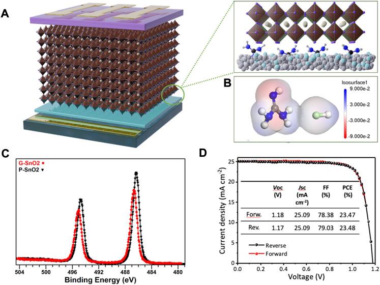
FIGURE 1. (A) Solar cell device architecture consisting of ITO/G-SnO2/perovskite/spiro-OMeTAD/Au, and G-SnO2/perovskite interface (inset). (B) Calculated ESP profiles of guanidinium chloride. (C) XPS analysis of Sn 3d region of G-SnO2 layer. (D) The best photovoltaic performance characteristics of PSCs using G-SnO2 ETLs annealed at a low temperature of 80°C.
Figure 1D shows the J/V curves of the champion device employing the G-SnO2 ETL, which yielded the best PCE of 23.48% with a VOC of 1.18 V, a short-circuit current density (JSC) of 25.1 mA/cm2 and a fill factor (FF) of 78.4%. The integrated JSC obtained from the EQE measurement was 24.69 mA/cm2 for the device, which is in accordance with the value determined from the J/V scan (Fig. S2). Compared with the reference device PCE of 20.91% (Supplementary Table S1), the performance showed a 12.3% enhancement with suppressed hysteresis, which can be attributed to improved electron transport in the ETL and fewer electron accumulation at the interfaces of the ETL.
The structural properties of the SnO2 ETL were first studied employing grazing incidence X-ray diffraction (GIXRD). At a low incident angle ω of 0.2° the signals related to the SnO2 crystallites were observed with distinct diffraction peaks at 25.95°, 33.31° and 50.82° (Supplementary Figure S3A) whose positions are coherent with the tetragonal rutile structure of SnO2 (ref. ICDD PDF 01-071-5,323). When increasing the incident angle ω from 0.2° to 0.4°, the ITO peaks became visible due to the larger depth probed, making it easy to distinguish them from the SnO2-related peaks. Compared with P-SnO2, films of G-SnO2 showed no difference in the peak positions (Supplementary Figure S3B), confirming that Gua-Cl doping does not change the structural properties of the ETL. Next, ultraviolet photoelectron spectroscopy (UPS) was carried out to analyze the energy level positions of P-SnO2 and G-SnO2. The work functions (Φ) of P-SnO2 and G-SnO2 were estimated from the secondary electron cutoff as −4.23 and −4.41 eV, respectively (Figure 2A). Plotting the UPS near the Fermi levels (EF) allowed calculating the valence band maxima (VBM) with respect to EF (−3.73 and −3.69 eV for G/P-SnO2) (Figure 2B), resulting in of EVB = −8.14 and −7.92 eV vs. vacuum level, respectively (cf. Supplementary Figure S6). Notably, the Fermi level of the G-SnO2 is situated deeper than that of the intrinsic P-SnO2 layer, suggesting n-type doping and leading to a slight band bending at the interface with the perovskite layer. Figure 2C shows Tauc plots of each SnO2 film on glass substrates. The optical bandgap values of G-SnO2 and P-SnO2 were deduced as 3.90 and 3.88 eV, respectively, i.e., essentially unchanged after doping. From these results, and combined with the conduction band minimum (CBM) of CsFAMA perovskites of −4.05 eV calculated by Abate and coworkers, (Wang et al., 2020b), an energy level diagram was constructed as shown in Figure 2D. As one important feature, an energy offset at the ETL/perovskite interface of 0.19 eV is obtained with G-SnO2, while P-SnO2 results in a flat alignment. Therefore, electron extraction is enhanced with G-SnO2 because of the higher energetic driving force, (Song et al., 2017), and a gradient-type band alignment between the perovskite layer and ITO is achieved.
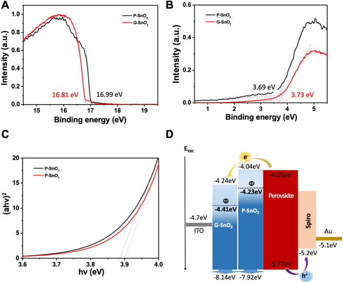
FIGURE 2. (A, B) UPS measurements on the pristine (P-SnO2) and guanidine doped (G-SnO2) films deposited on ITO, (A) secondary edge region; (B) Fermi level determination. (C) Tauc plot of P-SnO2 and G-SnO2 films deposited on ITO glass. (D) Energy level diagram derived from photoelectron and UV-vis absorption spectroscopy.
The morphology of the perovskite absorber layer was studied by SEM. It can be seen from Figures 3A, B that the perovskite films on P-SnO2 layers have crystallite sizes of around 200–400 nm, while much larger sizes of 500–800 nm were formed on G-SnO2 layers, leading to the grain size distributions depicted in Supplementary Figure S7. As visible in the cross-section view, the perovskite films grown on both types of SnO2 showed densely packed, highly crystalline grains (Figure 3D). The differences observed between the two cases clearly demonstrate the direct influence of the underlying ETL layer, generating nucleation centers and promoting perovskite growth, on the crystalline quality of the perovskite film as has been shown in many literature examples (Bouchard et al., 2017; Dunlap-Shohl et al., 2019; Medjahed et al., 2020). The different morphology of the perovskite films having the same thickness (Figure 3C, D) leads to a slight increase in the absorption of the layer grown on G-SnO2 (Supplementary Figure S8), which is beneficial for enhancing Jsc. This behavior is in accordance with reported results comparing the light absorption properties of perovskite thin films constituted of different grain sizes. (Xiao et al., 2014).
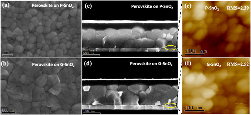
FIGURE 3. (A–D) SEM top and cross-section view of the perovskite layer grown on P- and G-SnO2, respectively (E, F) AFM images of the tin oxide surface w/wo Gua-Cl doping (scale bar: 100 nm).
To assess the surface morphology and roughness of the underlying ETL layer, atomic force microscopy (AFM) measurements were conducted. As shown in Figure 3F, the roughness of the G-SnO2 film (RMS = 2.52 nm) is slightly larger than that (2.39 nm) of the P-SnO2 film (cf. Supplementary Table S3), but the G-SnO2 film shows a denser surface morphology with improved homogeneity. The upper perovskite layer exhibited a reduced RMS roughness (cf. Supplementary Table S4), from 23.6 nm grown on a P-SnO2 film to 16.3 nm on G-SnO2. It can therefore be concluded that guanidine hydrochloride doped SnO2 favors the formation of a dense and smooth perovskite layer which is beneficial for the subsequent deposition of the HTL. Moreover, the large crystallite size contributes to the suppression of trap states generated at grain boundaries.
X-ray diffraction patterns of the perovskite layers on the different ETLs (Figure 4A) exhibit the main peaks located at 14.06°, 28.43°, and 31.84°, which are assigned to the (001), (002), and (012) reflections of the cubic crystalline phase of CsFAMA (space group m-3m). A strong diffraction peak at 12.68° originates from excess PbI2 used in the perovskite preparation, which is known to passivate the grain boundaries. (Parida et al., 2021). Perovskite growth on P-SnO2 resulted in a lattice constant of 6.278 (2) Å, while growth on G-SnO2 led to a slightly decreased value of 6.274 (2) Å, as visible by the shift of the diffraction peaks to larger angles (Figure 4B). Figure 4C depicts the evolution of the (00l) peak family for perovskites on P-SnO2 and G-SnO2 ETLs (cf. Supplementary Table S5). Due to the non-negligible contribution of the instrumental resolution to the broadening of the Bragg peaks, a quantitative analysis was not possible. However, considering that the crystallite size is >100 nm as determined from SEM analyses, the observed increased FWHM of the diffraction peaks denotes the presence of distortion (strain) in the lattice for both types of ETL. Importantly, the smaller FWHM increase observed for the perovskite grown on G-SnO2 is a sign of reduced strain and improved crystalline quality compared to the perovskite layer on P-SnO2.
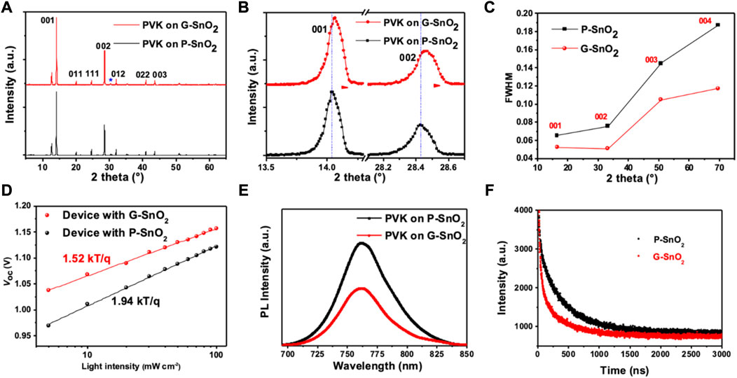
FIGURE 4. (A, B) XRD diffraction patterns of perovskite films prepared on P-/G-SnO2 layer (PVK: perovskite). (C) Evolution of the width (FWHM) of the (00l) perovskite diffraction peaks. (D) VOC as a function of the incident light intensity of devices based on P-/G-SnO2 ETL substrates. (E) steady-state photoluminescence (PL) spectra; (F) PL decay curves of the perovskite film deposited on P-/G-SnO2.
To further study the influence of the observed perovskite morphology and strain on the carrier recombination processes, we investigated the incident light intensity dependence of VOC (Figure 4D). If the slope of VOC versus light intensity is greater than kT/q (q: electron charge, k: Boltzmann constant, T: Kelvin temperature), VOC is strongly dependent on the incident light intensity and additional recombination caused by strain is involved. Here, the P-SnO2 devices exhibit a slope of 1.94 kT/q, while G-SnO2 devices show a significantly smaller value (1.52 kT/q), indicating that trap-assisted recombination was effectively inhibited by reduced strain, which is consistent with the fitted recombination resistance from electrochemical impedance spectroscopy (Supplementary Figure S9). This assumption is further supported by steady-state and time-resolved photoluminescence (TRPL) spectroscopy, as shown in Figure 4E. In both cases, the perovskite film gives rise to a broad PL signal peaking at 762 nm, but the PL intensity of the film grown on the G-SnO2 ETLs is significantly lower than that involving P-SnO2, which is a sign of enhanced electron injection. Analysis of the TRPL data (Figure 4F) results in a shorter excited state lifetime for the ITO/G-SnO2/perovskite stack (τ = 318 ns) than for the sample comprising the P-SnO2 ETL (τ = 415 ns), demonstrating the faster electron extraction from the perovskite film in the former case. Taken together, these data demonstrate that doping of the ETL with Gua-Cl leads to reduced charge accumulation and recombination losses at the perovskite/SnO2 interface, which is highly beneficial for solar cell performance.
To assess the reproducibility of the PSCs, we tested 25 devices using each type of ETL (Figure 5A). All solar cell parameters of the devices incorporating G-SnO2 are improved, while the main contribution stems from enhanced JSC (23.4 vs. 24.9 mA/cm2), originating from the concomitant reduction of the trap state density and the modulated band structure as discussed above. The statistical analysis yields an average and champion PCE of 22.86% and 23.48%, respectively, compared to 19.85% and 20.91% for the P-SnO2 cells. These results demonstrate the high reproducibility and effectiveness of the employed strategy. Figure 5B exhibits the stabilized power output at the maximum power point (MPP) in a nitrogen-filled glovebox, and no change was visible after MPP tracking for 120 s for both types of PSC. The stabilized PCE of the G-SnO2-based cell is 23.2%, in agreement with the PCE obtained from the J/V curve. Finally, the stability of the non-encapsulated PSCs was studied under a dry air environment (Figure 5C). The G-SnO2-based devices retained 96.1% of their initial PCE after 1,250 h, while the PCE of the P-SnO2 based PSCs shrank to 89.9% under the same conditions. The observed stability enhancement is ascribed to the enhanced carrier extraction capacity of G-SnO2 and the improved perovskite crystalline quality.
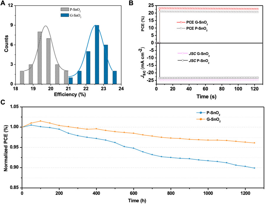
FIGURE 5. (A) Statistical distribution of the PCE of PSCs prepared with P-SnO2 and G-SnO2 (25 devices in each group). (B) Steady-state photocurrent density and device efficiency at maximum power point under continuous AM 1.5G illumination. (C) PCE decrease under dry air atmosphere of a reference device comprising the P-SnO2 ETL and of a device with G-SnO2 measured over a period of 1,250 h.
4 Conclusion
In summary, we presented a simple strategy for enhancing the performance of planar PSCs by doping the SnO2 ETL with guanidinium chloride. The observed improvements are related to both the modification of the ETL intrinsic properties and the enhancement of the crystalline quality of the perovskite layer. More specifically, the modified G-SnO2 ETL exhibited higher electron mobility and reduced defect state density than the pristine P-SnO2 ETL, resulting in reduced interfacial charge carrier recombination. In addition, G-SnO2 has a better-matched band alignment with the perovskite absorber further fostering efficient charge extraction. On the other hand, favored by the interaction between the guanidinium cation and halide anions from the perovskite precursors, the use of G-SnO2 also induces the growth of a perovskite layer exhibiting significantly increased grain size (around 600 nm vs. 300 nm) and lower strain, while maintaining a dense packing and smooth surface. As a result of this synergistic behavior, the PSCs using G-SnO2 exhibited an average PCE enhancement of 3% compared to devices with P-SnO2, reaching a maximum value of 23.48%. Combined with appealing stability and the possibility of low-temperature (80°C) processing, the proposed strategy also facilitates the realization of PSCs on flexible substrates and their integration into tandem devices.
Data availability statement
The original contributions presented in the study are included in the article/Supplementary Material, further inquiries can be directed to the corresponding authors.
Author contributions
PR and JY conceived the study and JY, YLi, AAM, SP, and DA performed the experiments. All authors contributed to the data interpretation. The manuscript was drafted by PR, JY, and YLiu, and all authors read and approved it.
Acknowledgments
Part of this work was realized on the Hybrid-En facility of SyMMES, and Etienne Omnes is thanked for experimental support. Benjamin Grévin is thanked for his valuable help with AFM analyses. The authors acknowledge the French Research Agency ANR for financial support (Grant PERSIL ANR-16-CE05-0019-02), and the LABEX Lanef (ANR-10-LABX-51-01) for its support with mutualized instrumentation. The PhD thesis of YLi was funded by UGA IDEX (project IRS C-Super), which is gratefully acknowledged.
Conflict of interest
The authors declare that the research was conducted in the absence of any commercial or financial relationships that could be construed as a potential conflict of interest.
Publisher’s note
All claims expressed in this article are solely those of the authors and do not necessarily represent those of their affiliated organizations, or those of the publisher, the editors and the reviewers. Any product that may be evaluated in this article, or claim that may be made by its manufacturer, is not guaranteed or endorsed by the publisher.
Supplementary material
The Supplementary Material for this article can be found online at: https://www.frontiersin.org/articles/10.3389/fmats.2023.1118641/full#supplementary-material
References
Anaraki, E. H., Kermanpur, A., Steier, L., Domanski, K., Matsui, T., Tress, W., et al. (2016). Highly efficient and stable planar perovskite solar cells by solution-processed tin oxide. Energy and Environ. Sci. 9, 3128–3134. doi:10.1039/c6ee02390h
Bouchard, M., Hilhorst, J., Pouget, S., Alam, F., Mendez, M., Djurado, D., et al. (2017). Direct evidence of chlorine-induced preferential crystalline orientation in methylammonium lead iodide perovskites grown on TiO2. J. Phys. Chem. C 121, 7596–7602. doi:10.1021/acs.jpcc.6b11529
Bu, T., Li, J., Zheng, F., Chen, W., Wen, X., Ku, Z., et al. (2018). Universal passivation strategy to slot-die printed SnO2 for hysteresis-free efficient flexible perovskite solar module. Nat. Commun. 9, 4609. doi:10.1038/s41467-018-07099-9
Chandrasekhar, P. S., Kumar, N., Swami, S. K., Dutta, V., and Komarala, V. K. (2016). Fabrication of perovskite films using an electrostatic assisted spray technique: The effect of the electric field on morphology, crystallinity and solar cell performance. Nanoscale 8, 6792–6800. doi:10.1039/c5nr08350h
Deng, K., Chen, Q., and Li, L. (2020). Modification engineering in SnO2 electron transport layer toward perovskite solar cells: Efficiency and stability. Adv. Funct. Mater. 30, 2004209. doi:10.1002/adfm.202004209
Dunlap-Shohl, W. A., Zhou, Y., Padture, N. P., and Mitzi, D. B. (2019). Synthetic approaches for halide perovskite thin films. Chem. Rev. 119, 3193–3295. doi:10.1021/acs.chemrev.8b00318
Fu, L., Li, H., Wang, L., Yin, R., Li, B., and Yin, L. (2020). Defect passivation strategies in perovskites for an enhanced photovoltaic performance. Energy and Environ. Sci. 13, 4017–4056. doi:10.1039/d0ee01767a
Grancini, G., Srimath Kandada, A. R., Frost, J. M., Barker, A. J., De Bastiani, M., Gandini, M., et al. (2015). Role of microstructure in the electron–hole interaction of hybrid lead halide perovskites. Nat. Photonics 9, 695–701. doi:10.1038/nphoton.2015.151
Huang, C., Lin, P., Fu, N., Sun, K., Ye, M., Liu, C., et al. (2018). Ionic liquid modified SnO2 nanocrystals as a robust electron transporting layer for efficient planar perovskite solar cells. J. Mater. Chem. A 6, 22086–22095. doi:10.1039/c8ta04131h
Ishibashi, H., Katayama, M., Tanaka, S., and Kaji, T. (2017). Hybrid perovskite solar cells fabricated from guanidine hydroiodide and tin iodide. Sci. Rep. 7, 4969. doi:10.1038/s41598-017-05317-w
Jalebi, M. A., Garmaroudi, Z. A., Cacovich, S., Stavrakas, C., Philippe, B., Richter, J. M., et al. (2018). Maximizing and stabilizing luminescence from halide perovskites with potassium passivation. Nature 555, 497–501. doi:10.1038/nature25989
Jiang, C.-S., Yang, M., Zhou, Y., To, B., Nanayakkara, S. U., Luther, J. M., et al. (2015). Carrier separation and transport in perovskite solar cells studied by nanometre-scale profiling of electrical potential. Nat. Commun. 6, 8397. doi:10.1038/ncomms9397
Jiang, Q., Zhang, L., Wang, H., Yang, X., Meng, J., Liu, H., et al. (2016). Enhanced electron extraction using SnO2 for high-efficiency planar-structure HC(NH2)2PbI3-based perovskite solar cells. Nat. Energy 2, 16177. doi:10.1038/nenergy.2016.177
Jiang, Q., Zhao, Y., Zhang, X., Yang, X., Chen, Y., Chu, Z., et al. (2019). Surface passivation of perovskite film for efficient solar cells. Nat. Photonics 13, 460–466. doi:10.1038/s41566-019-0398-2
Jodlowski, A. D., Roldán-Carmona, C., Grancini, G., Salado, M., Ralaiarisoa, M., Ahmad, S., et al. (2017). Large guanidinium cation mixed with methylammonium in lead iodide perovskites for 19% efficient solar cells. Nat. Energy 2, 972–979. doi:10.1038/s41560-017-0054-3
Jung, K.-N., Jung, J.-H., Im, W. B., Yoon, S., Shin, K.-H., and Lee, J.-W. (2013). Doped lanthanum nickelates with a layered perovskite structure as bifunctional cathode catalysts for rechargeable metal–air batteries. ACS Appl. Mater. Interfaces 5, 9902–9907. doi:10.1021/am403244k
Ke, W., Fang, G., Liu, Q., Xiong, L., Qin, P., Tao, H., et al. (2015). Low-temperature solution-processed tin oxide as an alternative electron transporting layer for efficient perovskite solar cells. J. Am. Chem. Soc. 137, 6730–6733. doi:10.1021/jacs.5b01994
Lee, Y., Paek, S., Cho, K. T., Oveisi, E., Gao, P., Lee, S., et al. (2017). Enhanced charge collection with passivation of the tin oxide layer in planar perovskite solar cells. J. Mater. Chem. A 5, 12729–12734. doi:10.1039/c7ta04128d
Liu, G., Zhong, Y., Feng, W., Yang, M., Yang, G., Zhong, J. X., et al. (2022). Multidentate chelation heals structural imperfections for minimized recombination loss in lead-free perovskite solar cells. Angew. Chem. Int. Ed. 61, e202209464. doi:10.1002/anie.202209464
Medjahed, A. A., Dally, P., Zhou, T., Lemaitre, N., Djurado, D., Reiss, P., et al. (2020). Unraveling the formation mechanism and ferroelastic behavior of MAPbI3 perovskite thin films prepared in the presence of chloride. Chem. Mater. 32, 3346–3357. doi:10.1021/acs.chemmater.9b04239
Murugadoss, G., Kanda, H., Tanaka, S., Nishino, H., Ito, S., Imahori, H., et al. (2016). An efficient electron transport material of tin oxide for planar structure perovskite solar cells. J. Power Sources 307, 891–897. doi:10.1016/j.jpowsour.2016.01.044
Odunmbaku, G. O., Chen, S., Guo, B., Zhou, Y., Ouedraogo, N. A. N., Zheng, Y., et al. (2022). Recombination pathways in perovskite solar cells. Adv. Mater. Interfaces 9, 2102137. doi:10.1002/admi.202102137
Parida, B., Jin, I. S., and Jung, J. W. (2021). Dual passivation of SnO2 by tetramethylammonium chloride for high-performance CsPbI2Br-based inorganic perovskite solar cells. Chem. Mater. 33, 5850–5858. doi:10.1021/acs.chemmater.1c00098
Qin, P., Zhang, J., Yang, G., Yu, X., and Li, G. (2019). Potassium-intercalated rubrene as a dual-functional passivation agent for high efficiency perovskite solar cells. J. Mater. Chem. A 7, 1824–1834. doi:10.1039/c8ta09026b
Ren, X., Yang, D., Yang, Z., Feng, J., Zhu, X., Niu, J., et al. (2017). Solution-Processed Nb:SnO2 electron transport layer for efficient planar perovskite solar cells. ACS Appl. Mater. Interfaces 9, 2421–2429. doi:10.1021/acsami.6b13362
Song, S., Kang, G., Pyeon, L., Lim, C., Lee, G.-Y., Park, T., et al. (2017). Systematically optimized bilayered electron transport layer for highly efficient planar perovskite solar cells (η = 21.1%). ACS Energy Lett. 2, 2667–2673. doi:10.1021/acsenergylett.7b00888
Sutanto, A. A., Caprioglio, P., Drigo, N., Hofstetter, Y. J., Garcia-Benito, I., Queloz, V. I. E., et al. (2021). 2D/3D perovskite engineering eliminates interfacial recombination losses in hybrid perovskite solar cells. Chem 7, 1903–1916. doi:10.1016/j.chempr.2021.04.002
Tu, B., Shao, Y., Chen, W., Wu, Y., Li, X., He, Y., et al. (2019). Novel molecular doping mechanism for n-doping of SnO(2) via triphenylphosphine oxide and its effect on perovskite solar cells. Adv. Mater. 31, e1805944. doi:10.1002/adma.201805944
Wang, P., Li, R., Chen, B., Hou, F., Zhang, J., Zhao, Y., et al. (2020). Gradient energy alignment engineering for planar perovskite solar cells with efficiency over 23%. Adv. Mater. 32, 1905766. doi:10.1002/adma.201905766
Wang, P., Wang, J., Zhang, X., Wang, H., Cui, X., Yuan, S., et al. (2018). Boosting the performance of perovskite solar cells through a novel active passivation method. J. Mater. Chem. A 6, 15853–15858. doi:10.1039/c8ta05593a
Wang, Q., Zu, F., Caprioglio, P., Wolff, C. M., Stolterfoht, M., Li, M., et al. (2020). Large conduction band energy offset is critical for high fill factors in inorganic perovskite solar cells. ACS Energy Lett. 5, 2343–2348. doi:10.1021/acsenergylett.0c00980
Wu, S., Li, Z., Zhang, J., Liu, T., Zhu, Z., and Jen, A. K.-Y. (2019). Efficient large guanidinium mixed perovskite solar cells with enhanced photovoltage and low energy losses. Chem. Commun. 55, 4315–4318. doi:10.1039/c9cc00016j
Xiao, Z., Dong, Q., Bi, C., Shao, Y., Yuan, Y., and Huang, J. (2014). Solvent annealing of perovskite-induced crystal growth for photovoltaic-device efficiency enhancement. Adv. Mater. 26, 6503–6509. doi:10.1002/adma.201401685
Xiong, Z., Chen, X., Zhang, B., Odunmbaku, G. O., Ou, Z., Guo, B., et al. (2022). Simultaneous interfacial modification and crystallization control by biguanide hydrochloride for stable perovskite solar cells with PCE of 24.4%. Adv. Mater. 34, 2106118. doi:10.1002/adma.202106118
Ye, J., Li, Y., Medjahed, A. A., Pouget, S., Aldakov, D., Liu, Y., et al. (2021). Doped bilayer tin(IV) oxide electron transport layer for high open-circuit voltage planar perovskite solar cells with reduced hysteresis. Small 17, e2005671. doi:10.1002/smll.202005671
Yu, M., Chen, L., Li, G., Xu, C., Luo, C., Wang, M., et al. (2020). Effect of guanidinium chloride in eliminating O2− electron extraction barrier on a SnO2 surface to enhance the efficiency of perovskite solar cells. RSC Adv. 10, 19513–19520. doi:10.1039/d0ra01501f
Zhang, S., Gu, H., Chen, S.-C., and Zheng, Q. (2021). KF-Doped SnO2 as an electron transport layer for efficient inorganic CsPbI2Br perovskite solar cells with enhanced open-circuit voltages. J. Mater. Chem. C 9, 4240–4247. doi:10.1039/d1tc00277e
Zhang, W., Xiong, J., Li, J., and Daoud, W. A. (2019). Guanidinium induced phase separated perovskite layer for efficient and highly stable solar cells. J. Mater. Chem. A 7, 9486–9496. doi:10.1039/c9ta01893j
Zhao, P., Kim, B. J., and Jung, H. S. (2018). Passivation in perovskite solar cells: A review. Mater. Today Energy 7, 267–286. doi:10.1016/j.mtener.2018.01.004
Keywords: perovskite solar cells, electron transport layer, SnO2, guanidinium chloride, grain size
Citation: Ye J, Li Y, Medjahed AA, Pouget S, Aldakov D, Liu Y and Reiss P (2023) Enhanced performance of planar perovskite solar cells by doping the SnO2 electron transport layer with guanidinium chloride. Front. Mater. 10:1118641. doi: 10.3389/fmats.2023.1118641
Received: 07 December 2022; Accepted: 17 February 2023;
Published: 02 March 2023.
Edited by:
Hui Tong, Central South University, ChinaReviewed by:
Anurag Krishna, Interuniversity Microelectronics Centre (IMEC), BelgiumChenxin Ran, Northwestern Polytechnical University, China
Copyright © 2023 Ye, Li, Medjahed, Pouget, Aldakov, Liu and Reiss. This is an open-access article distributed under the terms of the Creative Commons Attribution License (CC BY). The use, distribution or reproduction in other forums is permitted, provided the original author(s) and the copyright owner(s) are credited and that the original publication in this journal is cited, in accordance with accepted academic practice. No use, distribution or reproduction is permitted which does not comply with these terms.
*Correspondence: Jiajiu Ye, eWVqaWFqaXVAbWFpbC51c3RjLmVkdS5jbg==; Yueli Liu, bHlsbGl1d2h1dEB3aHV0LmVkdS5jbg==; Peter Reiss, cGV0ZXIucmVpc3NAY2VhLmZy