 Keqiang Li
 Yeqiang Bu1
- 1Center for X-Mechanics, Zhejiang University, Hangzhou, China
- 2ZJU-Hangzhou Global Scientific and Technological Innovation Center, Zhejiang University, Hangzhou, China
Over the past few decades, in situ transmission electron microscopy (TEM) has emerged as a powerful experimental technique for materials design and characterization. It offers unparalleled dynamic details of materials deformation under mechanical stimuli, providing fundamental insights into their deformation and failure mechanisms for various materials. In this review, we summarize recent advances on in situ TEM mechanical characterization techniques, including classical tension holders, nanoindentation holders, MEMS devices, thermal bimetallic-based techniques, and nanomanipulation techniques. The advantages and limitations of in situ TEM tests are also discussed. To provide a broader perspective, the article highlights promising opportunities for in situ TEM mechanical testing studies in characterization-processing-manufacturing based on nanomanipulation, ultrafast TEM, electron beam irradiation environmental conditions, data-driven machine learning, and integrated experimental and simulation characterization. This article aims to provide a comprehensive understanding of in situ TEM-based mechanical characterization techniques to promote the development of novel materials with improved mechanical properties for various applications.
1 Introduction
Accurately characterizing and understanding materials’ microscale deformation mechanisms is crucial for optimizing their macroscopic mechanical performance. Since the investigation of crystal dislocations in 1956 (Hirsch et al., 1956), TEM has been widely applied for the structure-property study of materials (Meyers et al., 2006; Zhu and Li, 2010; Zhu et al., 2012; An et al., 2019; Pan et al., 2021; Li et al., 2022a; Zhu and Wu, 2022). Experimentally, the most viable approach for microstructural analysis relies on ex situ studies. However, they only provide a glimpse of the structure after deformation is complete, missing critical intermediate structural insights concerning the deformation process. This is particularly relevant to nanoscale phenomenon such as dislocation nucleation and propagation (Zheng et al., 2010a; Bu et al., 2019), dislocation/nanoprecipitates interactions (Yang et al., 2021a; Yang et al., 2021b), dislocation/boundary interactions (Kacher et al., 2014; Li et al., 2022b), deformation twinning (Wang et al., 2017a; Sun et al., 2022), phase transformation (Wang et al., 2020a; Fu et al., 2022), and GB-mediated plasticity (Wang et al., 2017b; Zhu et al., 2021). To capture the dynamic evolution of microstructures during deformation, nanomechanical testing systems integrated into TEM has become paramount, such as classical tension method, nanoindentation techniques, micromechanical and microelectromechanical system (MEMS) devices, and nanomanipulation techniques. Up to now, TEM-based in situ nanomechanical testing methods have opened new horizons for directly characterizing and analyzing dynamic mechanical behaviors at the atomic scale (Yu et al., 2015; Minor and Dehm, 2019; Zheng and Mao, 2021). They have been used for in situ testing of tension (Oh et al., 2009; Rupert et al., 2009), compression (Imrich et al., 2015), indentation (Minor et al., 2006; Wang et al., 2010a), shearing (Oviedo et al., 2015; Zhu et al., 2019), and bending (Bai et al., 2007; Xu et al., 2020) of materials within TEM, with real-time visualization of deformation mechanisms. When forces can also be measured, these methods allow for a fundamental understanding of the constitutive behavior of materials at the nanoscale.
To advance in situ TEM capabilities for direct observation of materials’ structural evolution under real-time loading conditions and promote further development of TEM-based in situ mechanical testing, this review focuses on the advanced techniques currently applied in the field of TEM-based in situ nanomechanical characterization. Specifically, classical tension holders, nanoindentation holders, MEMS devices, thermal bimetallic-based techniques, and nanomanipulation techniques are covered, and their advanced features and limitations in typical applications are discussed. Finally, we provide perspectives on the general challenges and potential research capabilities of in situ TEM, with particular emphasis on exploiting the latest developments in TEM mechanical testing in characterization-processing-manufacturing based on nanomanipulation, ultrafast TEM, electron beam irradiation environmental conditions, data-driven machine learning, and integrated experimental and simulation characterization.
2 In situ TEM mechanical tests based on classical tension holders
One of the most basic mechanical tests involves the uniaxial tension of a sample with concurrent measurements of load and strain. Given the constraints imposed by the ultra-high vacuum and limited space within the pole-pieces of TEM, the most intuitive approach towards replicating this test within a TEM environment would be the construction of a suitable tensile device. Based on this premise, in the 1960s and 1970s, research on the dynamics of dislocations in metals facilitated the development of devices and led to the emergence of a series of in situ tensile TEM holders designs (Wilsdorf, 1958; Berghezan and Fourdeux, 1959; Fisher, 1959; Forsyth and Wilson, 1960; Pashley, 1960; Takahashi et al., 1960), all based on the fundamental principle of fixing one end of the sample and connecting the other end to the moving part of the holder to achieve uniaxial tensile displacement loading of the sample.
Up to now, Gatan Inc. has developed commercial straining holders (Gatan 654), as illustrated in Figure 1A (Legros, 2014). In practical experiments, the sample is either shaped using focused ion beam (FIB) or affixed to a deformable grid that is compatible with the holder fixation system (i.e., pin, screw, clamp). This sample is then stretched at a constant rate from a long rigid shaft attached to a worm gear box actuated by an electric motor and located in a housing outside TEM. Due to its simple structure, the Gatan 654 uniaxial straining holder can achieve significant sample displacement and strain using an electric motor, and is often employed for observing the evolution of the microstructure within local regions of a sample (Nie and Wang, 2011; Matsukawa and Liu, 2012; Kai et al., 2013). For example, Zhang et al. (2015) utilized the Gatan 654 holder to investigate the unique fracture behavior of CrMnFeCoNi high-entropy alloys. By subjecting the CrMnFeCoNi sample to in situ tensile deformation, the formation process of cracks was observed, as shown in Figure 1B. Bu et al. (2021) also utilized the Gatan 654 holder to study the dynamic interaction between local chemical fluctuations and dislocations in high-entropy alloys, as shown in Figure 1C. These dynamic findings significantly improved the understanding of plastic deformation mechanisms at the nanoscale and hold important implications for establishing structure-property relations in materials.
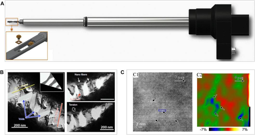
FIGURE 1. (A) A classic tensile holder manufactured by Gatan Inc. (Legros, 2014). (B) Crack bridging via near-tip twinned nanobridges in the CrMnFeCoNi high-entropy alloy (Zhang et al., 2015). (C) Local chemical fluctuations induced dislocation pinning in a HfNbTiZr high-entropy alloys under loading (Bu et al., 2021).
In addition, the in situ straining at room temperature can be augmented by additional heating or cooling capabilities, enabling researchers to investigate the nanomechanical behavior of materials at high or low temperatures (Fang et al., 2021; Wang et al., 2021). Cooling is achieved by connecting a cold finger to a liquid helium or nitrogen reservoir at the end of the sample holder. On the other hand, heating is facilitated by a miniaturized furnace, which can attain temperatures of up to 1,000°C, depending on the furnace’s material and the gap between the TEM pole pieces. However, the large size and mass of the furnace leads to slow heating rates, and the entire system requires a considerable amount of time to stabilize to eliminate thermal drifts at high temperatures.
While the classical tensile holders have been used to study the microstructural deformation mechanisms of various materials at different temperatures, this method has limitations in terms of displacement control accuracy, stability, and the lack of force sensors to quantitatively measure loading force during deformation. These limitations make it difficult to observe and characterize deformation processes at higher resolutions, as well as quantitatively analyze them. Moreover, the front-end stretching mechanism’s large space requirements and interference during motion limit the technique’s ability to achieve double-tilt, which hinders its ability to characterize low-index crystallographic orientations of crystalline materials with high resolution.
3 In situ TEM mechanical tests based on nanoindentation holders
Nanoindentation technology is commonly used for measuring the elastic modulus and hardness of materials. The step-like and discontinuous curve of the load-depth obtained through nanomechanical indentation corresponds to different deformation mechanisms, revealing the discreteness of microplastic deformation (Schuh, 2006; Golovin, 2021). By incorporating nanoindentation into TEM, it is possible to observe in situ the morphological changes of material microstructures during the indentation process. The in situ TEM nanoindentation device was first introduced by Lawrence Berkeley National Laboratory (Wall and Dahmen, 1998; Stach et al., 2001) and subsequently utilized to dynamically observe the microstructural evolution during nanomechanical indentation. Minor et al. (2001) performed the first quantitative characterized the indentation behavior of aluminum film samples deposited on a silicon substrate. Building upon the developed in situ nanoindentation technology, Hysitron Corporation optimized and introduced the PI95 nanoindentation sample holder for commercial use. As shown in Figure 2A, the front end of the sample holder is a diamond probe indenter movable end capable of X/Y/Z three-degree-of-freedom motion, and the sample is fixed on the opposite end of the indenter (Wang et al., 2017c). Through the piezoelectric module inside the holder, the movable end can be accurately displaced to contact the sample and apply load for real-time observation of sample deformation. At the same time, the classic driving sensor and capacitance displacement sensor connected to the movable end of the indenter can quantitatively measure the force-displacement curve during loading, which helps to deepen the understanding of the relationship between material micro-deformation and mechanical properties.
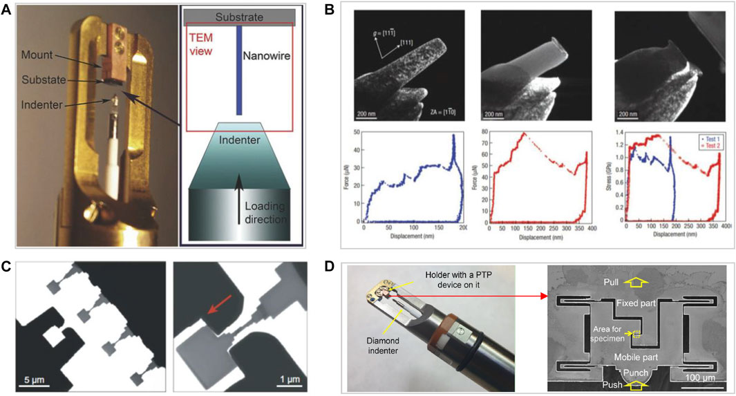
FIGURE 2. (A) The Hysitron PI 95 TEM PicoIndenter and the corresponding schematic of a compression test (Wang et al., 2017c). (B) Two consecutive in situ TEM compression tests on a FIB microfabricated 160-nm-top-diameter nickel pillar with <111> orientation (Shan et al., 2008). (C) The microfabricated diamond bridge samples and corresponding diamond tensile gripper (Dang et al., 2021a). (D) Push-to-Pull device and the working area of the Hysitron PI 95 TEM Picoindenter holder (Loginov et al., 2021).
For example, Shan et al. (2008) conducted in situ weak-beam dark-field TEM loading experiments on submicron single-crystal nickel pillars with diameter of 160 nm, revealing, for the first time the phenomenon of dislocation escape during in situ compression, as shown in Figure 2B. Liu et al. (2019a) utilized the nanoindentation holder to conduct in situ uniaxial compression testing on magnesium single crystal samples and quantitatively obtained the stress-strain response data for the sample. In addition, through the design of special sample and indenter shapes, Dang et al. (2021a) used the Hysitron PI95 nanoindentation holder to achieve in situ uniaxial tensile testing of single crystal diamonds. As shown in Figure 2C, standard single crystal diamond tensile samples were prepared using FIB technology, along with a “concave” shaped tensile clamping device. The diamond sample was placed in the “T” shape end of the clamping device and subjected to reverse loading to achieve in situ uniaxial tension of the single crystal diamond. A more general method of converting compression force into tension is to use so-called “Push-to-pull” (PTP) devices (Ding et al., 2016; Dang et al., 2021b), often made from silicon using lithography techniques, as shown in Figure 2D (Loginov et al., 2021). However, this technique is extremely time-consuming and requires long milling times or specific lithography techniques (Jennings and Greer, 2011).
Recently, several advanced options have been developed to enhance the capabilities of the nanoindentation holder. One example is the use of a piezoelectric actuator for lateral actuation, enabling in situ studies of tribology, wear, and friction (Jacobs and Carpick, 2013; Hintsala et al., 2017; Bhowmick et al., 2019). Another option involves superimposing an oscillation onto quasi-static loading, can be used for in situ fatigue testing (Bufford et al., 2016). Additionally, an electrical PTP device has been developed, allowing for simultaneous current-voltage characterization of a material (Bhowmick et al., 2013; Wang et al., 2015a). Based on the self-designed MEMS device, Bernal et al. (2014) investigated the relationship between resistance and strain of Ag and Si nanowires. These advancements in the nanoindentation holder have expanded the range of possibilities for material characterization and analysis.
As mentioned above, researchers have successfully conducted in situ TEM experiments on various nano-scale specimens using the PI95 nanoindentation sample holder. These experiments encompass indentation, compression, and tension (employing either PTP devices or specially designed tension clamps) tests. Additionally, advanced options like lateral actuation, oscillation superimposition, and electrical characterization have further augmented the capabilities of nanoindentation holders, thereby broadening the scope of material analysis and characterization. However, the PI95 sample holder suffers from a limited range of piezoelectric fine adjustment, often requiring mechanical coarse adjustment, which has poor displacement control accuracy and can easily lead to specimen damage during experimentation. Additionally, the maximum output force of the PI95 sample holder is insufficient for mechanical loading experiments on large and brittle materials. Furthermore, the PI95 sample holder is still unable to achieve double-tilt. These limitations of the PI95 sample holder need to be addressed for further advancement in the field of materials science.
4 In situ TEM mechanical tests based on MEMS techniques
Currently, various MEMS-based stages have been developed for in situ mechanical testing in TEM, each with different designs and operating principles. Typically, MEMS-based TEM mechanical testing devices can be classified into two categories: passive MEMS technology, which requires external loading to drive the device, such as the PTP devices combined with a nanoindentation TEM holder (Guo et al., 2011; Jiang et al., 2016; Loginov et al., 2022) and the co-fabrication of the sample with its testing frame, which can avoid micromanipulation (harvesting, welding) of micro- and nano-samples (wires, fiber, films). For instance, a U-spring-shaped Si structure supporting a nanocrystalline Al film processed using vapor deposition has been fabricated and successfully tested using a simple straining holder (Mompiou et al., 2013). However, they all require external loading to drive the device and cannot provide accurate mechanical feedback information.
Another type is active MEMS technology, which combines driving and sensing capabilities into one device. Many researchers have made efforts and explorations on its application of in situ mechanical characterization in TEM. For example, Zhu et al. developed a MEMS tensile sample holder based on V-shaped electrothermal beams (Zhu and Espinosa, 2005). As shown in Figure 3A, the MEMS chip is mounted on the front end of the sample holder and fixed on the chip holder through two clamps. When an injected current passes through the V-shaped Si beams, they expand and impose a uniaxial tensile displacement to the shuttles on which samples are mounted. The Si combs are attached to Si beams with known stiffness that serve as load sensors. The typical loads are in the range of μN, while the displacement remains very limited, rarely above a couple of micrometers. The system capabilities are demonstrated by the in situ TEM testing of polysilicon films (Espinosa et al., 2007), ZnO nanowires (Agrawal et al., 2009), and carbon nanotubes (Peng et al., 2008). However, it is worth noting that the front end of the sample rod of this device is almost occupied by the wire bonding posts, limiting its double-tilt function.
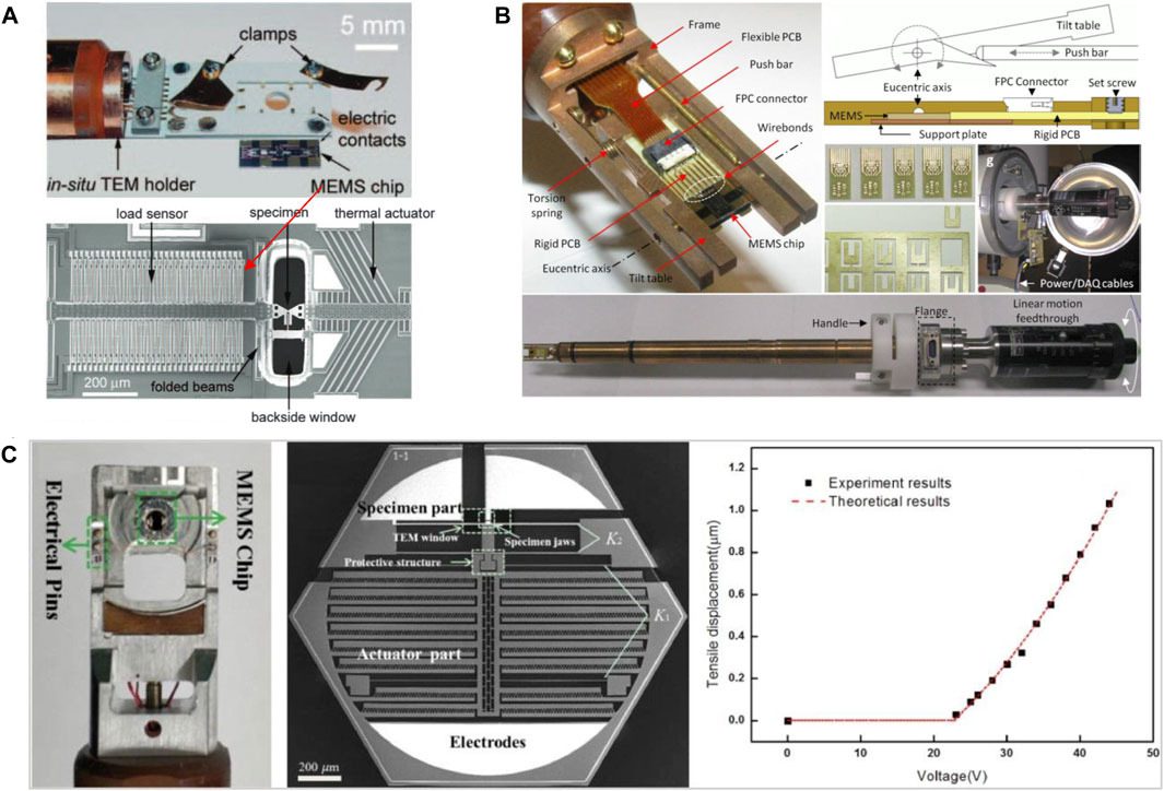
FIGURE 3. (A) In TEM tensile testing device including actuator, load sensor, and specimen (Zhu and Espinosa, 2005). (B) Schematics and pictures of the double-tilt holder (Bernal et al., 2015). (C) Pictures of the holder tip with the tensile device, SEM micrographs of the electrostatic actuated chip and the tensile displacement-voltage curves of the chip (Yang et al., 2019).
To address the issue of double-tilt, Espinosa’s team further developed a double-tilt in situ TEM holder based on a MEMS mechanical platform (Bernal et al., 2015), as illustrated in Figure 3B. The tilting table has an inclined surface in contact with a moving bar. A torsion spring pushes the tilting table against the push bar to maintain contact. The push rod is further connected to a manual knob that provides precise linear motion via an internal connecting rod within the holder. By pushing the push rod back and forth, the tilting table is tilted. However, the limited radial size of the sample holder’s front end is occupied by the inclined surface and torsion spring mechanisms, while the lead wire method of the sample holder occupies a significant axial size space at the front end. Therefore, the developed mechanical sample holder is only applicable to JEOL TEM. In addition, due to the limitation of high working temperature, electrothermal MEMS devices cannot be widely used in assembling temperature-sensitive objects or in low-temperature fields.
Regarding electrostatic MEMS actuators (Volland et al., 2002; Beyeler et al., 2007), they have two different structures in terms of transverse and lateral comb drives. Compared to electrothermal MEMS actuators, they possess some capabilities such as high frequency response, low power consumption, and no hysteresis, making them the choice for TEM mechanical sample holders. For instance, Yang et al. (2019) designed an electrostatic actuated tensile device, as shown in Figure 3C. Through specific shape and structure design, the device can be installed on the Gatan 646 double-tilt TEM holder. To demonstrate its performance, in situ tensile testing for penta-twinned silver nanowires was conducted in a high-resolution TEM. Meanwhile, an accurate tensile stress-strain curve was obtained, as shown in Figure 3C. The experimental results show that the device can achieve a tilt angle of 10° around both X and Y axes when conducting in situ tensile testing experiments.
In conclusion, the utilization of MEMS-based platforms has gained significant popularity in nanomechanical testing due to their ability to exert precise control over the deformation process and provide quantitative measurements of displacements and forces. Moreover, these platforms readily allow for the integration of multiple fields, such as electric and thermal fields, facilitating a more comprehensive understanding of mechanical properties. Notably, Han and others recently devised a high-temperature in situ observation method, enabling the examination of atomic-scale deformation processes in nanomaterials (Zhang et al., 2021). However, most of these MEMS platforms heavily rely on quite complicated setups, making their implementation and operation challenging and expensive (Lu et al., 2011).
5 In situ TEM mechanical tests based on thermal bimetallic based techniques
Based on the thermal bimetallic technique, Han’s group developed an innovative in situ tensile testing device for TEM (Zhang et al., 2007). As shown in Figure 4A, this technique consists of two metal strips with different coefficients of thermal expansion. When heated, the bimetallic strips bend towards the side with the smaller coefficient of expansion, allowing for the manipulation of the sample by changing the orientation of the strips. This technique can slowly and gently deform the testing samples while retaining the double-tilt capability for in situ atomic-scale observations (Wang et al., 2010b; Han et al., 2010). By utilizing this device, Wang et al. (2014) conduct in situ tensile experiments on platinum thin films and discovered that the plasticity mechanism transitions from cross-grain dislocation glide to coordinated rotation of multiple grains as the grain size decreases, as shown in Figure 4B. Additionally, Liu et al. (2019b) used this device to study the atomic-scale tensile and fracture behavior of nanoporous gold thin films, while Lu et al. (2016) conducted this in situ tensile tests on body-centered cubic molybdenum nanowires and found a significant dependence of its plasticity on aspect ratio and size. Furthermore, the bi-metallic extensor can function as a double-tilt deformation stage with precise displacement control. This innovation has been successfully commercialized by BestronST. A recent study conducted by Wang et al. (2022) demonstrated the application of this approach in an in situ investigation at atomic resolution. The study focused on elucidating the mechanisms underlying sliding-dominant deformation at general tilt grain boundaries (GBs) in platinum bicrystals. The researchers observed two distinct processes: direct atomic-scale sliding along the GB and sliding accompanied by atom transfer across the boundary plane (Wang et al., 2022).
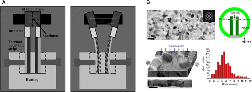
FIGURE 4. (A) Schematic illustration of the tensile tool prior to extensile experiment with the SiC nanowires scattered on the manipulator, and the conducting tensile experiment on the SiC nanowires (Zhang et al., 2007). (B) In situ tensile pulling of the platinum thin film in a TEM using the thermal bimetallic techniques (Wang et al., 2014).
It should be noted that the bimetallic strips technique enables atomic-scale mechanical testing, but the loading of stress relies on the bending deformation of the strips, which cannot guarantee uniaxial loading of the sample. Moreover, due to the bimetallic strips were fixed on the copper-ring grid with superglue, making this method cannot be used for high temperature in situ deformation.
6 In situ TEM mechanical tests based on nanomanipulation techniques
Nanomanipulation is a technique used to manipulate and position nanostructures for the assembly of nano devices (Du et al., 2006). This method allows for flexible maneuvering and precise positioning, making it ideal for device prototyping and property tuning. It has been extensively utilized in scanning electron microscopy to realize simultaneous imaging and direct interactions with nanoscaled samples (Shi et al., 2016; Jiang et al., 2017). In the following sections, we will introduce the application of nanomanipulation in TEM, focusing on two perspectives: conventional nanomanipulation techniques and nanomanipulation coupled with 3D reconstruction techniques.
6.1 Conventional nanomanipulation techniques
The first nanomanipulation experiment was performed by Eigler and Schweizer using a scanning tunneling microscope (STM) to form the IBM logo by positioning individual xenon atoms on a nickel substrate (Eigler and Schweizer, 1990). STM has since been integrated into TEM specimen holders for in situ scanning probe microscopy probing of nm-scale features with simultaneous two-dimensional TEM observations. For example, Andrén et al. (1974) used six piezoelectric ceramic rings as driving elements to perform in situ tensile experiments on electrochemically etched molybdenum wires. In 1996, Naitoh et al. installed a piezoelectric ceramic scanning tube on the sample holder to achieve X/Y/Z three-dimensional nanomanipulation of the sample, and used mechanical driving to achieve a large stroke of 2 mm in the X direction, enabling in situ STM characterization under TEM (Naitoh et al., 1996). In 2003, Svensson et al. used a sticky drive mechanism to achieve large stroke precision manipulation in the x, y, and z directions on a TEM sample holder using a piezoelectric ceramic scanning tube, and obtained in situ STM images of highly oriented pyrolitic graphite (Svensson et al., 2003), as shown in Figure 5A. Based on these developments, Nanofactory Instrument AB and Zeptools further optimized and developed TEM-STM sample holders for commercial use.
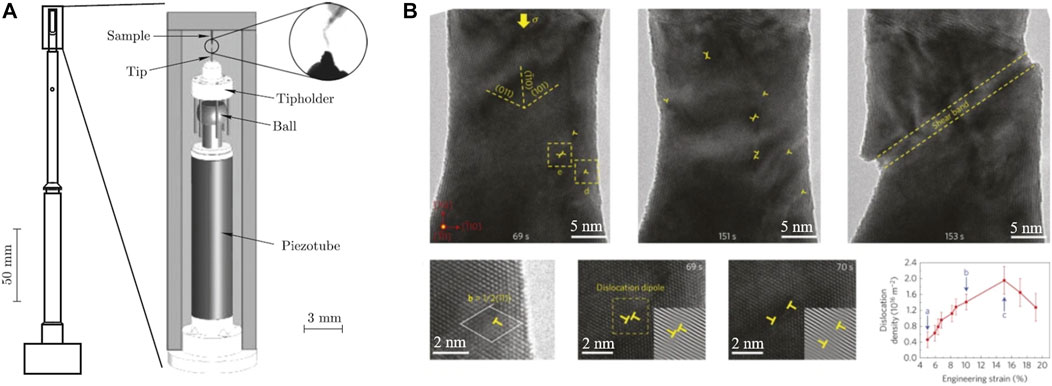
FIGURE 5. (A) Schematic illustration of the side-entry holder and its STM head with a three-dimensional coarse motion mechanism. The inset shows a TEM image of a carbon nanotube (about 20 nm in diameter) which has been selectively approached, in situ, with a gold tip (Svensson et al., 2003). (B) Dislocation dynamics inside a tungsten bicrystal nanowire under compression (Wang et al., 2015b).
For the TEM-STM specimen holder, a miniature STM is built into the TEM specimen holder, incorporating a compact 3-axis inertial sliding mechanism with piezoelectric actuator (Svensson et al., 2003; Larsson et al., 2004). This manipulator has the advantages of compact structure, fast response, and high displacement control precision (∼1 nm), which reduces the rigid motion component of the sample during loading, resulting in high mechanical stability and adaptability to the confined sample chamber environment of the TEM. By utilizing the high-frequency periodic bending and stretching of a piezoelectric ceramic tube with four electrodes by a ceramic ball, the mobile end can generate a large range of three-dimensional spatial displacement. Combined with piezoelectric manipulation, high-precision displacement motion can be achieved.
A methodology for sequential in situ fabrication and nanomechanical testing has been developed based on the STM-TEM holder, which provides an ideal platform for atomistic insights into deformation behaviors. For example, Lu et al. (2010) used the nanomanipulation function of the STM-TEM holder to bring two gold single crystal nanowires, each with a diameter of approximately 5 nm and located at the fixed and active ends, into lateral contact. Without heating, the two nanowires were mechanically welded to form a complete single crystal nanowire. And then, in situ tensile experiments of the single crystal gold nanowires were carried out by driving the active end of the nanomanipulation sample holder (Lu et al., 2010). To further enhance weldability, it is a common practice to apply a constant voltage at the nanoscale tip of the probe when it contacts with the sample on the side fixed to the substrate (Zhong et al., 2017; Cao et al., 2018). This in situ thermal welding technique allows for direct fabrication of high-quality metallic nanowires in TEM (Zhong et al., 2014; Wang et al., 2018). These procedures produce bridge-shaped single crystals with clean surfaces, controllable orientations, and varying dimensions. Additionally, after the nanowelding process, in situ nanomechanical testing, including tension (Wang et al., 2020b), compression (He et al., 2020), and shear (Zhu et al., 2020a; Zhu et al., 2020b), can be instantly carried out via the precise displacement control of the probe. As shown in Figure 5B, Wang et al. (2015b) successfully prepared tungsten nanowires with diameters less than 20 nm using the in situ welding method, and achieved real-time loading and deformation observation of the tungsten nanowires with atomic resolution, revealing for the first time the twinning-dominated plastic deformation behavior and pseudo-elastic phenomenon in body-centered cubic single crystal tungsten.
Furthermore, for TEM-STM sample holders with nanomanipulation capabilities, a specialized atomic force microscopy (AFM) chip can be attached to the tip of the sample holder to sense ultra-small forces and simultaneously image the real-time material deformation, as shown in Figure 6A (Lu et al., 2011). Each AFM chip consists of a cantilever with a unique spring constant, determined by the geometry of the tip. Conducting tests within the TEM enables the precise determination of cantilever deflection and sample deformation, including elongation, compression, and bending, as shown in Figure 6B (Liu et al., 2013). The deflection output of the cantilever is collected by a computer and plotted against the probe’s movement to produce a force-versus-distance diagram, as illustrated in Figure 6C. Additionally, real-time imaging in HRTEM allows for the observation of sample deformation (Figure 6D).
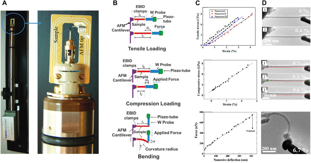
FIGURE 6. (A) The TEM-AFM holder manufactured by Nanofactory Instrument AB (Lu et al., 2011). (B) Schematics showing the application of AFM cantilever for in situ TEM mechanical testing under: tensile, compressive, and bending loads, and (C) the corresponding force-deflection curve and (D) real-time HRTEM snapshots for the deformation of a nanowire (Liu et al., 2013).
6.2 Nanomanipulation coupled with 3D reconstruction techniques
For the nanomanipulation sample holder developed by Nanofactory Instrument AB and Zeptools, there is a serious motion coupling problem in the X/Y/Z directions due to the point contact friction between the end cap and the ceramic ball, which increases the difficulty of nanomanipulation. To address the aforementioned issues, Wang’s group has developed a double-tilt in situ TEM sample holder, referred to as XNano, which is capable of mechanical loading and has five manipulation parameters in the X/Y/Z/α/β dimensions (Zhang et al., 2020a; Zhang et al., 2020b), as shown in Figure 7A. The sample holder’s movements in the five degrees of freedom are precisely driven by three groups of piezoelectric actuators to minimize the artifacts caused by vibration and drifting of the TEM stage. The manipulation of α-rotation is accomplished by accumulating step-lengths using a stick-slip drive mechanism, which enables 360° rotational displacement of the ceramic spindle within the piezoelectric shear slice. Consequently, the XNano sample holder can autonomously rotate 360° without using the TEM goniometer, effectively addressing the vibration drift issue caused by the goniometer’s rotation and the missing wedge angle issue due to incomplete angle rotation in 3D reconstruction (Midgley and Weyland, 2003). Similarly, based on the stick-slip drive mechanism, the holder can achieve a 3 mm displacement stroke and 0.1 μm displacement accuracy in the X-direction. Stage II completes the fine adjustments in the X-direction and rough and fine adjustments in the Y/Z-direction. The Stage II module consists of a piezoelectric ceramic tube, ceramic balls, and front and back pressure plates. Based on the inverse piezoelectric effect of the piezoelectric ceramic tube connecting the ceramic ball, the module achieves precise X/Y/Z manipulation by applying voltage to cause small deformation of the piezoelectric ceramic tube. The precise adjustment stroke in the X direction is 1 μm with displacement accuracy <0.1 nm, while the precise adjustment stroke in the Y/Z direction is 7 μm with displacement accuracy <0.1 nm. Furthermore, by applying periodic voltage signals and utilizing the stick-slip drive mechanism between the piezoelectric ceramic tube and the front and back pressure plates, rough adjustments in the Y/Z-direction can be achieved with a displacement stroke of up to 2 mm and a displacement accuracy of 0.1 μm. For in situ loading experiments, the X-direction motion stability directly affects the deformation process. The compact two-stage driving module of the XNano TEM sample holder avoids the displacement coupling problem between the X-direction rough adjustment manipulation and the Y/Z-directions, and the X-direction nanomanipulation has a small mechanical hysteresis with excellent stability. Regarding the Y/Z-direction rough adjustment manipulation, the frictional contact between the Y-Z module’s linear contact surface in Stage II greatly reduces the influence of gravity on manipulation stability. Additionally, Stage III integrates a piezoelectric stack and a fan-shaped driver on the ceramic ball’s front pressure plate based on the stick-slip drive mechanism, allowing β-tilt manipulation (±10°) to achieve good atomic-scale resolution. In short, the XNnao sample holder combines 3D reconstruction technology of TEM with in situ experimental techniques based on nanomanipulation. This enables in situ three-dimensional structural analysis at different loading stages to investigate the evolution mechanism of the sample material.
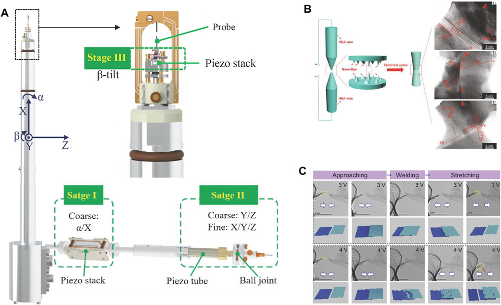
FIGURE 7. (A) The XNano holder and detail schematic for the nano-piezo manipulator with three-stage (Zhang et al., 2020a; Zhang et al., 2020b). (B) Preparation of nano-junctions with different load/twin boundary orientations (Liang et al., 2021). (C) In-situ TEM electrical joule thermal welding and tensile experiments of graphene sheets (Liu et al., 2018).
Using the XNano sample holder, Liang et al. (2021) developed an in situ welding method for Al0.1CoCrFeNi high-entropy alloy samples with nanoscale (10–20 nm) dimensions in TEM and achieved controllable adjustment of the twin orientation in the nanoscale sample, as shown in Figure 7B. And the in situ tensile tests were performed on the nanoscale samples to reveal the anisotropy of plastic deformation and fracture modes in high-entropy alloy nanotwin samples. Additionally, as shown in Figure 7C using this device, Liu et al. (2018) conducted in situ electro-thermal welding and mechanical tensile tests on graphene layers, revealing that the high-quality electro-thermal welding interface between macroscopic graphene elements originated from the high interfacial binding force induced by covalent bonding between graphene layers across the interface. This work provides a new strategy for manufacturing high-melting-point graphene components (Liu et al., 2018).
Furthermore, to quantitatively characterize the mechanical behavior of samples in TEM, AFM chips of different specifications can be integrated at the front end of the XNano sample holder (Figure 8A). Combined with its own nanomanipulation accuracy in the five degrees of freedom, it can support the acquisition of high-resolution in situ images of mechanical behavior of crystalline materials at low indices, while providing a load of up to 200 mN. For example, Nie et al. (2019) successfully achieved high-precision manipulation of diamond nanoneedles at sub-nanometer levels in TEM by pressing the nanoneedle tip against the diamond head to conduct bending experiments, as illustrated in Figure 8B. They discovered that as the size of the nanoneedle tip decreased, the maximum achievable tensile strength and elastic strain increased. Additionally, utilizing the XNano in situ system in TEM, Nie et al. performed precise loading on diamond nanopillars and observed the dynamic behavior of internal dislocations during compression, revealing the widespread room-temperature dislocation plasticity in diamond, as shown in Figure 8C (Nie et al., 2020). Based on the 3D TEM imaging technology provided by XNano, Nie et al. characterized the 3D morphology of dislocations in diamond, and through detailed calibration of the dislocation types and slip planes, they revealed that dislocations in diamond tend to slip on the non-close-packed {100} planes, overturning the long-standing textbook understanding that dislocations in the diamond lattice should slip on the close-packed {111} planes. In addition, Zhang et al. (2022) conducted in situ compression experiments on covalently bonded silicon nitride (Si3N4) ceramics nanopillars in TEM using the XNano holder, as shown in Figure 8D. In the experiment, the nanopillars were mounted on the nanomanipulator end of the XNano mechanical platform and then precisely driven against a diamond flat punch. The uniaxial compression was carried out in displacement-controlled mode with a nominal strain rate of 10-3/s at room temperature. The stress-strain curve during the in situ compression process of the nanopillars was obtained by the AFM chip, revealing unprecedented room-temperature compressive plastic deformation.
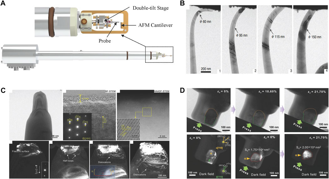
FIGURE 8. (A) The XNano holder integrated AFM Cantilever. (B) The maximum deformation immediately before the fracture during sequentially breaking the diamond nanoneedle for its high aspect ratio geometry (Nie et al., 2019). (C) Evolution of a Diamond Nanopillar during Compression (Nie et al., 2020). (D) Bright-field images of a nanopillar at different compression strains revealed by in situ TEM; the orange and green dashed lines show the outlines of the α and ß grains, respectively, with coherent interfaces; outside of the dashed lines in the nanopillar are the Si3N4 grains bonded by the glass phase (Zhang et al., 2022).
In summary, the use of nanomanipulation technology in STM-TEM sample holder enables the preparation of high-quality nanoscale samples, and facilitates various mechanical loading and high-resolution characterization under TEM. Furthermore, equipped with an AFM chip, STM-TEM sample holder provides crucial quantitative data on stress-strain relationships during mechanical loading, enabling a quantitative study of material mechanical behavior at the nanoscale. Furthermore, the combined application of nanomanipulation and 3D reconstruction techniques can facilitate the exploration of real-time 3D evolution of nanomaterials under external loads, enabling quasi-4D TEM characterization that provides deeper insights into microscale deformation mechanisms of materials.
7 Summary and outlook
This paper presents a comprehensive review of the technical advancements in various in situ TEM mechanical experimental techniques. Such experiments reveal unique properties of nanomaterials and provide useful images or videos that assist researchers in analyzing underlying mechanisms, thus enhancing their potential applications. Nevertheless, despite significant progress, in situ TEM characterization encounters several key challenges:
(1) In situ TEM nanomanipulator-based techniques with integrated force sensors have been utilized to study the interfacial properties of layered 2D materials (Li et al., 2018), such as molybdenum disulfide, via in situ TEM nanomechanical cleavage of atomic layers (Tang et al., 2014). In addition, Schweizer et al. (2020) have reported on an in situ mechanical cleaning method that allows for the targeted removal of contamination from both sides of two-dimensional membranes down to atomic-scale cleanliness based on the nanomanipulator-based techniques. Meanwhile, the mechanisms of re-contamination can be revealed through TEM characterization. In addition, as mentioned earlier, nanomanipulation technology can also be used for the manufacture of nanoscale samples. Therefore, significant innovative efforts are required to develop integrated characterization, processing, and manufacturing techniques based on nanomanipulation technology in TEM.
(2) Recent developments in ultrafast TEM (UTEM) have enabled investigate materials at extremely short spatial and temporal resolutions by integrating the excellent spatial resolution of TEM with the temporal resolution of ultrafast femtosecond laser-based spectroscopy (Zewail, 2010; Browning et al., 2012; Plemmons et al., 2015; Zhu et al., 2020c), which is very suitable for studying dynamic processes. Currently, ultrafast TEM has been employed to investigate non-equilibrium structural phase transitions (Park et al., 2009), transient structures (Barwick et al., 2008), and complex mechanical phenomena at the nanoscale (Flannigan et al., 2009), providing new insights for materials science research. However, further efforts are needed to explore the potential integration of these techniques with in situ mechanical testing methods.
(3) Electron beam irradiation can induce various effects on materials, including localized sample heating (Stangebye et al., 2022), and creation of defects/artifacts (Sarkar et al., 2015). These effects can potentially alter the mechanical properties of the specimen in the observed deformation behavior (Zheng et al., 2010b; Zang et al., 2011). To address these challenges, the current approach primarily focuses on minimizing the electron dose and exposure time during testing (Filleter et al., 2011; Liu et al., 2012; Qu and Deng, 2017). Additionally, the use of thermally conductive probes/sample holders is desirable to enhance heat dissipation. Furthermore, the rapid development of UTEM technology in recent years has provided essential hardware support in this regard. It is important to note that the exact methodology to eliminate or minimize the electron beam irradiation effects may vary depending on the specific experimental setup and materials under investigation. Therefore, it is essential to carefully consider the trade-off between minimizing the electron beam effects and obtaining meaningful in situ TEM mechanical testing results.
(4) Given the complex service environments of materials, external conditions such as temperature and electricity must be considered. This adds an additional challenge for the in situ TEM device to accommodate both stress and temperature or electricity, which has been demonstrated to be feasible, particularly with MEMS-based devices (Zhang et al., 2021) and laser-beam-induced heating (Grosso et al., 2020). However, more innovative work is still needed in this area. Besides, there is a lack of research on TEM-based nanomechanical characterization techniques at ultra-low temperatures. Therefore, more work is needed to explore the underlying mechanisms and to develop the necessary technology.
(5) The in situ TEM results, particularly the time-lapse videos captured during in situ studies, generate a wealth of data. Recently, artificial intelligence techniques, specifically machine learning, have been successfully applied to the in situ TEM characterization of energy materials (Zheng et al., 2022; Wang et al., 2023). Such techniques offer great assistance in analyzing TEM images of nanomaterials in terms of their defects, morphology, structure, and spectra (Cheng et al., 2022), which can reveal material mechanisms and facilitate the design and development of new materials. However, there is still much work to be done in exploring how to integrate machine learning and big data technologies with in situ mechanical characterization of TEM to extract hidden information from vast amounts of experimental data.
(6) Combining in situ TEM deformation experiments and atomistic simulations bridges gaps between structure and energetics, signal and information, and across time and length scales (Kacher et al., 2019). Therefore, integrated in situ TEM experiments and atomistic simulations with high precision and high fidelity will enable a deep and fundamental understanding of defect mechanics (Dingreville et al., 2016), providing a mechanistic basis for designing high-performance materials for advanced structural applications (Sangid, 2020). But it still requires exploration in order to get greater and deeper integration between atomistic simulations and in situ TEM experiments.
In conclusion, in situ TEM mechanical tests provide valuable insights into the relationships between material structure, properties, and mechanisms under various external conditions. By utilizing the high spatial and temporal resolution capabilities of TEM and integrating various advanced techniques, in situ TEM enables the unprecedented visualization of atomic-scale dynamic processes in both conventional and advanced materials under external loading. Continued advances in both hardware and software developments are expected to yield even smaller, more precise, and versatile in situ TEM testing techniques for material characterization, allowing for enhanced control over material properties and performance, and facilitating the development and application of new materials.
Author contributions
KL and HW carried out the structure of the article and wrote the paper, YB revised and edited the manuscript. All authors contributed to the article and approved the submitted version.
Funding
This work was supported by the National Natural Science Foundation of China (11725210, 11672355, and 11702165).
Conflict of interest
The authors declare that the research was conducted in the absence of any commercial or financial relationships that could be construed as a potential conflict of interest.
Publisher’s note
All claims expressed in this article are solely those of the authors and do not necessarily represent those of their affiliated organizations, or those of the publisher, the editors and the reviewers. Any product that may be evaluated in this article, or claim that may be made by its manufacturer, is not guaranteed or endorsed by the publisher.
References
Agrawal, R., Peng, B., and Espinosa, H. D. (2009). Experimental-computational investigation of ZnO nanowires strength and fracture. Nano Lett. 9 (12), 4177–4183. doi:10.1021/nl9023885
An, X. H., Wu, S. D., Wang, Z. G., and Zhang, Z. F. (2019). Significance of stacking fault energy in bulk nanostructured materials: Insights from Cu and its binary alloys as model systems. Prog. Mat. Sci. 101, 1–45. doi:10.1016/j.pmatsci.2018.11.001
Andrén, H. O., Loberg, B., and Nordén, H. (1974). A low strain rate tensile holder for the electron microscope. J. Phys. E Sci. Instr. 7 (4), 316–317. doi:10.1088/0022-3735/7/4/030
Bai, X. D., Golberg, D., Bando, Y., Zhi, C. Y., Tang, C. C., Mitome, M., et al. (2007). Deformation-driven electrical transport of individual boron nitride nanotubes. Nano Lett. 7 (3), 632–637. doi:10.1021/nl062540l
Barwick, B., Park, H. S., Kwon, O. H., Baskin, J. S., and Zewail, A. H. (2008). 4D imaging of transient structures and morphologies in ultrafast electron microscopy. Science 322 (5905), 1227–1231. doi:10.1126/science.1164000
Berghezan, A., and Fourdeux, A. (1959). Transmission electron microscopy studies of the mechanism of plastic deformation. J. Appl. Phys. 30 (12), 1913–1922. doi:10.1063/1.1735089
Bernal, R. A., Filleter, T., Connell, J. G., Sohn, K., Huang, J. X., Lauhon, L. J., et al. (2014). In situ electron microscopy four-point electromechanical characterization of freestanding metallic and semiconducting nanowires. Small 10 (4), 725–733. doi:10.1002/smll.201300736
Bernal, R. A., Ramachandramoorthy, R., and Espinosa, H. D. (2015). Double-tilt in situ TEM holder with multiple electrical contacts and its application in MEMS-based mechanical testing of nanomaterials. Ultramicroscopy 156, 23–28. doi:10.1016/j.ultramic.2015.04.017
Beyeler, F., Neild, A., Oberti, S., Bell, D. J., Sun, Y., Dual, J., et al. (2007). Monolithically fabricated microgripper with integrated force sensor for manipulating microobjects and biological cells aligned in an ultrasonic field. J. Microelectromechanical Syst. 16 (1), 7–15. doi:10.1109/JMEMS.2006.885853
Bhowmick, S., Hintsala, E., Stauffer, D., and Syed Asif, S. S. (2019). In situ TEM study of friction and wear of olivine. Microsc. Microanal. 25 (2), 1898–1899. doi:10.1017/S1431927619010225
Bhowmick, S., Stauffer, D., Guo, H., Kaps, S., Mishra, Y. K., Hrkac, V., et al. (2013). In situ electromechanical study of ZnO nanowires. Microsc. Microanal. 19 (2), 434–435. doi:10.1017/S1431927613004169
Browning, N. D., Bonds, M. A., Campbell, G. H., Evans, J. E., LaGrange, T., Jungjohann, K. L., et al. (2012). Recent developments in dynamic transmission electron microscopy. Curr. Opin. Solid State Mat. Sci. 16 (1), 23–30. doi:10.1016/j.cossms.2011.07.001
Bu, Y. Q., Li, Z. M., Liu, J. B., Wang, H. T., Raabe, D., and Yang, W. (2019). Nonbasal slip systems enable a strong and ductile hexagonal-close-packed high-entropy phase. Phys. Rev. Lett. 122 (7), 075502. doi:10.1103/PhysRevLett.122.075502
Bu, Y. Q., Wu, Y., Lei, Z. F., Yuan, X. Y., Wu, H. H., Feng, X. B., et al. (2021). Local chemical fluctuation mediated ductility in body-centered-cubic high-entropy alloys. Mat. Today 46, 28–34. doi:10.1016/j.mattod.2021.02.022
Bufford, D. C., Stauffer, D., Mook, W. M., Syed Asif, S. A., Boyce, B. L., and Hattar, K. (2016). High cycle fatigue in the transmission electron microscope. Nano Lett. 16 (8), 4946–4953. doi:10.1021/acs.nanolett.6b01560
Cao, G., Wang, J. W., Du, K., Wang, X. L., Li, J. X., Zhang, Z., et al. (2018). Superplasticity in gold nanowires through the operation of multiple slip systems. Adv. Funct. Mat. 28 (51), 1805258. doi:10.1002/adfm.201805258
Cheng, Z. H., Wang, C. L., Wu, X., and Chu, J. H. (2022). Review in situ transmission electron microscope with machine learning. J. Semicond. 43 (8), 081001. doi:10.1088/1674-4926/43/8/081001
Dang, C. Q., Chou, J. P., Dai, B., Chou, C. T., Yang, Y., Fan, R., et al. (2021a). Achieving large uniform tensile elasticity in microfabricated diamond. Science 371 (6524), 76–78. doi:10.1126/science.abc4174
Dang, C. Q., Lin, W. T., Meng, F. L., Zhang, H. T., Fan, S. F., Li, X. C., et al. (2021b). Enhanced tensile ductility of tungsten microwires via high-density dislocations and reduced grain boundaries. J. Mat. Sci. Technol. 95, 193–202. doi:10.1016/j.jmst.2021.04.021
Ding, M. S., Tian, L., Han, W. Z., Li, J., Ma, E., and Shan, Z. W. (2016). Nanobubble fragmentation and bubble-free-channel shear localization in helium-irradiated submicron-sized copper. Phys. Rev. Lett. 117 (21), 215501. doi:10.1103/PhysRevLett.117.215501
Dingreville, R., Karnesky, R. A., Puel, G., and Schmitt, J. H. (2016). Review of the synergies between computational modeling and experimental characterization of materials across length scales. J. Mat. Sci. 51, 1178–1203. doi:10.1007/s10853-015-9551-6
Du, E., Cui, H. L., and Zhu, Z. Q. (2006). Review of nanomanipulators for nanomanufacturing. Int. J. Nanomanuf. 1 (1), 83–104. doi:10.1504/IJNM.2006.011382
Eigler, D. M., and Schweizer, E. K. (1990). Positioning single atoms with a scanning tunnelling microscope. Nature 344, 524–526. doi:10.1038/344524a0
Espinosa, H. D., Zhu, Y., and Moldovan, N. (2007). Design and operation of a MEMS-based material testing system for nanomechanical characterization. J. Microelectromechanical Syst. 16 (5), 1219–1231. doi:10.1109/JMEMS.2007.905739
Fang, Y., Chen, Y. J., Chen, B., Li, S. Z., Gludovatz, B., Park, E. S., et al. (2021). An in situ ambient and cryogenic transmission electron microscopy study of the effects of temperature on dislocation behavior in CrCoNi-based high-entropy alloys with low stacking-fault energy. Appl. Phys. Lett. 27 (26), 261903. doi:10.1063/5.0069086
Filleter, T., Bernal, R., Li, S., and Espinosa, H. D. (2011). Ultrahigh strength and stiffness in cross-linked hierarchical carbon nanotube bundles. Adv. Mat. 23 (25), 2855–2860. doi:10.1002/adma.201100547
Fisher, R. M. (1959). Specimen holder for controlled deformation in the Elmiskop. Rev. Sci. Instrum. 30 (10), 925–926. doi:10.1063/1.1716385
Flannigan, D. J., Samartzis, P. C., Yurtsever, A., and Zewail, A. H. (2009). Nanomechanical motions of cantilevers: Direct imaging in real space and time with 4D electron microscopy. Nano Lett. 9 (2), 875–881. doi:10.1021/nl803770e
Forsyth, P. J. E., and Wilson, R. N. (1960). Device for straining and fracturing thin foil specimens inside an electron microscope. J. Sci. Instrum. 37 (1), 37–38. doi:10.1088/0950-7671/37/1/413
Fu, X. Q., Wang, X. D., Zhao, B. K., Zhang, Q. H., Sun, S. Y., Wang, J. J., et al. (2022). Atomic-scale observation of non-classical nucleation-mediated phase transformation in a titanium alloy. Nat. Mat. 21 (3), 290–296. doi:10.1038/s41563-021-01144-7
Golovin, Y. I. (2021). Nanoindentation and mechanical properties of materials at submicro-and nanoscale levels: Recent results and achievements. Phys. Solid State 63, 1–41. doi:10.1134/S1063783421010108
Grosso, R. L., Muccillo, E. N. S., Muche, D. N. F., Jawaharram, G. S., Barr, C. M., Monterrosa, A. M., et al. (2020). In situ transmission electron microscopy for ultrahigh temperature mechanical testing of ZrO2. Nano Lett. 20 (2), 1041–1046. doi:10.1021/acs.nanolett.9b04205
Guo, H., Chen, K., Oh, Y., Wang, K., Dejoie, C., Syed Asif, S. A., et al. (2011). Mechanics and dynamics of the strain-induced M1-M2 structural phase transition in individual VO2 nanowires. Nano Lett. 11 (8), 3207–3213. doi:10.1021/nl201460v
Han, X. D., Wang, L. H., Liu, P., Yue, Y. H., Yang, M. J., Sun, J. L., et al. (2010). Dynamic atomic mechanisms of plasticity of Ni nanowires and nano crystalline ultra-thin films. Mat. Sci. Forum 654-656, 2293–2296. doi:10.4028/www.scientific.net/MSF.654-656.2293
He, Y., Li, B., Wang, C. M., and Mao, S. X. (2020). Direct observation of dual-step twinning nucleation in hexagonal close-packed crystals. Nat. Commun. 11 (1), 2483. doi:10.1038/s41467-020-16351-0
Hintsala, E. D., Stauffer, D. D., Oh, Y., and Syed Asif, S. S. (2017). In situ TEM scratch testing of perpendicular magnetic recording multilayers with a novel MEMS tribometer. Jom 69, 51–56. doi:10.1007/s11837-016-2154-0
Hirsch, P. B., Horne, R. W., and Whelan, M. J. (1956). LXVIII. Direct observations of the arrangement and motion of dislocations in aluminium. Philos. Mag. 1 (7), 677–684. doi:10.1080/14786435608244003
Imrich, P. J., Kirchlechner, C., Kiener, D., and Dehm, G. (2015). In situ TEM microcompression of single and bicrystalline samples: Insights and limitations. Jom 67, 1704–1712. doi:10.1007/s11837-015-1440-6
Jacobs, T. D., and Carpick, R. W. (2013). Nanoscale wear as a stress-assisted chemical reaction. Nat. Nanotechnol. 8 (2), 108–112. doi:10.1038/nnano.2012.255
Jennings, A. T., and Greer, J. R. (2011). Tensile deformation of electroplated copper nanopillars. Philos. Mag. 91 (7-9), 1108–1120. doi:10.1080/14786435.2010.505180
Jiang, C. C., Lu, H. J., Zhang, H. T., Shen, Y. J., and Lu, Y. (2017). Recent advances on in situ SEM mechanical and electrical characterization of low-dimensional nanomaterials. Scanning 2017, 1–11. doi:10.1155/2017/1985149
Jiang, L., Hu, T., Yang, H., Zhang, D. L., Topping, T., Lavernia, E. J., et al. (2016). Deformation of a ceramic/metal interface at the nanoscale. Nanoscale 8 (20), 10541–10547. doi:10.1039/C6NR02011A
Kacher, J., Eftink, B. P., Cui, B., and Robertson, I. M. (2014). Dislocation interactions with grain boundaries. Curr. Opin. Solid State Mat. Sci. 18 (4), 227–243. doi:10.1016/j.cossms.2014.05.004
Kacher, J., Zhu, T., Pierron, O., and Spearot, D. E. (2019). Integrating in situ TEM experiments and atomistic simulations for defect mechanics. Curr. Opin. Solid State Mat. Sci. 23 (3), 117–128. doi:10.1016/j.cossms.2019.03.003
Kai, X. Z., Li, Z. Q., Fan, G. L., Guo, Q., Tan, Z. Q., Zhang, W. L., et al. (2013). Strong and ductile particulate reinforced ultrafine-grained metallic composites fabricated by flake powder metallurgy. Scr. Mat. 68 (8), 555–558. doi:10.1016/j.scriptamat.2012.11.024
Larsson, M. W., Wallenberg, L. R., Persson, A. I., and Samuelson, L. (2004). Probing of individual semiconductor nanowhiskers by TEM-STM. Microsc. Microanal. 10 (1), 41–46. doi:10.1017/S1431927604040176
Legros, M. (2014). In situ mechanical TEM: Seeing and measuring under stress with electrons. C. R. Phys. 15 (2-3), 224–240. doi:10.1016/j.crhy.2014.02.002
Li, S., Enami, T., Ohmura, T., and Tsurekawa, S. (2022b). Direct measurement of shear stress for dislocation transferring across {111} Σ3 grain boundary in aluminum bicrystal via in situ straining TEM. Scr. Mat. 221, 114953. doi:10.1016/j.scriptamat.2022.114953
Li, L. L., Zhang, Z. J., Zhang, P., and Zhang, Z. F. (2022a). A review on the fatigue cracking of twin boundaries: Crystallographic orientation and stacking fault energy. Prog. Mat. Sci. 10, 101011. doi:10.1016/j.pmatsci.2022.101011
Li, X., Sun, M., Shan, C. X., Chen, Q., and Wei, X. L. (2018). Mechanical properties of 2D materials studied by in situ microscopy techniques. Adv. Mat. Interfaces 5 (5), 1701246. doi:10.1002/admi.201701246
Liang, C. Y., Zhang, Q., Shao, Y. C., Bu, Y. Q., Liu, J. B., Li, X. Y., et al. (2021). Influence of load orientations with respect to twin boundaries on the deformation behaviors of high-entropy alloy nanocrystals. MRS Bull. 46, 205–216. doi:10.1557/s43577-021-00046-y
Liu, B. Y., Liu, F., Yang, N., Zhai, X. B., Zhang, L., Yang, Y., et al. (2019a). Large plasticity in magnesium mediated by pyramidal dislocations. Science 365 (6448), 73–75. doi:10.1126/science.aaw2843
Liu, P., Wei, X., Song, S. X., Wang, L. H., Hirata, A., Fujita, T., et al. (2019b). Time-resolved atomic-scale observations of deformation and fracture of nanoporous gold under tension. Acta Mater 165, 99–108. doi:10.1016/j.actamat.2018.11.022
Liu, F., Tang, D. M., Gan, H. B., Mo, X. S., Chen, J., Deng, S. Z., et al. (2013). Individual boron nanowire has ultra-high specific Young’s modulus and fracture strength as revealed by in situ transmission electron microscopy. ACS Nano 7 (11), 10112–10120. doi:10.1021/nn404316a
Liu, X. H., Wang, J. W., Liu, Y., Zheng, H., Kushima, A., Huang, S., et al. (2012). In situ transmission electron microscopy of electrochemical lithiation, delithiation and deformation of individual graphene nanoribbons. Carbon 50 (10), 3836–3844. doi:10.1016/j.carbon.2012.04.025
Liu, Y., Liang, C., Wei, A., Jiang, Y., Tian, Q., Wu, Y., et al. (2018). Solder-free electrical Joule welding of macroscopic graphene assemblies. Mat. Today Nano 3, 1–8. doi:10.1016/j.mtnano.2018.09.005
Loginov, P. A., Sidorenko, D. A., Orekhov, A. S., and Levashov, E. A. (2021). A novel method for in situ TEM measurements of adhesion at the diamond-metal interface. Sci. Rep. 11 (1), 10659. doi:10.1038/s41598-021-89536-2
Loginov, P. A., Zaitsev, A. A., Sidorenko, D. A., and Levashov, E. A. (2022). Effect of self-assembling WC film upon diamond on adhesion strength with Fe-Co-Ni binder: In situ TEM tensile tests. Scr. Mat. 208, 114331. doi:10.1016/j.scriptamat.2021.114331
Lu, D., Chen, H. B., Wu, J. S., and Chan, C. M. (2011). Direct measurements of the Young's modulus of a single halloysite nanotube using a transmission electron microscope with a bending stage. J. Nanosci. Nanotechnol. 11 (9), 7789–7793. doi:10.1166/jnn.2011.4720
Lu, Y., Huang, J. Y., Wang, C., Sun, S. H., and Lou, J. (2010). Cold welding of ultrathin gold nanowires. Nat. Nanotechnol. 5 (3), 218–224. doi:10.1038/nnano.2010.4
Lu, Y., and Lou, J. (2011). Quantitative in-situ nanomechanical characterization of metallic nanowires. Jom 63, 35–42. doi:10.1007/s11837-011-0155-6
Lu, Y., Xiang, S. S., Xiao, L. R., Wang, L. H., Deng, Q. S., Zhang, Z., et al. (2016). Dislocation “bubble-like-effect” and the ambient temperature super-plastic elongation of body-centred cubic single crystalline molybdenum. Sci. Rep. 6 (1), 22937. doi:10.1038/srep22937
Matsukawa, Y., and Liu, G. S. (2012). In situ TEM study on elastic interaction between a prismatic loop and a gliding dislocation. J. Nucl. Mat. 425 (1-3), 54–59. doi:10.1016/j.jnucmat.2011.12.001
Meyers, M. A., Mishra, A., and Benson, D. J. (2006). Mechanical properties of nanocrystalline materials. Prog. Mat. Sci. 51, 427–556. doi:10.1016/j.pmatsci.2005.08.003
Midgley, P. A., and Weyland, M. (2003). 3D electron microscopy in the physical sciences: The development of Z-contrast and EFTEM tomography. Ultramicroscopy 96 (3-4), 413–431. doi:10.1016/S0304-3991(03)00105-0
Minor, A. M., and Dehm, G. (2019). Advances in in situ nanomechanical testing. MRS Bull. 44 (6), 438–442. doi:10.1557/mrs.2019.127
Minor, A. M., Morris, J. W., and Stach, E. A. (2001). Quantitative in situ nanoindentation in an electron microscope. Appl. Phys. Lett. 79 (11), 1625–1627. doi:10.1063/1.1400768
Minor, A. M., Syed Asif, S. A., Shan, Z. W., Stach, E. A., Cyrankowski, E., Wyrobek, T. J., et al. (2006). A new view of the onset of plasticity during the nanoindentation of aluminium. Nat. Mat. 5 (9), 697–702. doi:10.1038/nmat1714
Mompiou, F., Legros, M., Boé, A., Coulombier, M., Raskin, J. P., and Pardoen, T. (2013). Inter-and intragranular plasticity mechanisms in ultrafine-grained Al thin films: An in situ TEM study. Acta Mater 61 (1), 205–216. doi:10.1016/j.actamat.2012.09.051
Naitoh, Y., Takayanagi, K., and Tomitori, M. (1996). Visualization of tip-surface geometry at atomic distance by TEM-STM holder. Surf. Sci. 357, 208–212. doi:10.1016/0039-6028(96)00094-5
Nie, A. M., Bu, Y. Q., Huang, J. Q., Shao, Y. C., Zhang, Y. Z., Hu, W. T., et al. (2020). Direct observation of room-temperature dislocation plasticity in diamond. Matter 2 (5), 1222–1232. doi:10.1016/j.matt.2020.02.011
Nie, A. M., Bu, Y. Q., Li, P. H., Zhang, Y. Z., Jin, T. Y., Liu, J. B., et al. (2019). Approaching diamond’s theoretical elasticity and strength limits. Nat. Commun. 10 (1), 5533. doi:10.1038/s41467-019-13378-w
Nie, A. M., and Wang, H. T. (2011). Deformation-mediated phase transformation in gold nano-junction. Mat. Lett. 65 (23-24), 3380–3383. doi:10.1016/j.matlet.2011.07.037
Oh, S. H., Legros, M., Kiener, D., and Dehm, G. (2009). In situ observation of dislocation nucleation and escape in a submicrometre aluminium single crystal. Nat. Mat. 8 (2), 95–100. doi:10.1038/nmat2370
Oviedo, J. P., Kc, S., Lu, N., Wang, J. G., Cho, K., Wallace, R. M., et al. (2015). In situ TEM characterization of shear-stress-induced interlayer sliding in the cross section view of molybdenum disulfide. ACS Nano 9 (2), 1543–1551. doi:10.1021/nn506052d
Pan, Q. S., Zhang, L. X., Feng, R., Lu, Q. H., An, K., Chuang, A. C., et al. (2021). Gradient cell-structured high-entropy alloy with exceptional strength and ductility. Science 374 (6570), 984–989. doi:10.1126/science.abj8114
Park, H. S., Kwon, O. H., Baskin, J. S., Barwick, B., and Zewail, A. H. (2009). Direct observation of martensitic phase-transformation dynamics in iron by 4D single-pulse electron microscopy. Nano Lett. 9 (11), 3954–3962. doi:10.1021/nl9032704
Pashley, D. W. (1960). A study of the deformation and fracture of single-crystal gold films of high strength inside an electron microscope. Proc. R. Soc. Lond. A. Math. Phys. Sci. 255 (1281), 218–231. doi:10.1098/rspa.1960.0064
Peng, B., Locascio, M., Zapol, P., Li, S. Y., Mielke, S. L., Schatz, G. C., et al. (2008). Measurements of near-ultimate strength for multiwalled carbon nanotubes and irradiation-induced crosslinking improvements. Nat. Nanotechnol. 3 (10), 626–631. doi:10.1038/nnano.2008.211
Plemmons, D. A., Suri, P. K., and Flannigan, D. J. (2015). Probing structural and electronic dynamics with ultrafast electron microscopy. Chem. Mat. 27 (9), 3178–3192. doi:10.1021/acs.chemmater.5b00433
Qu, X. L., and Deng, Q. S. (2017). Damage and recovery induced by a high energy e-beam in a silicon nanofilm. RSC Adv. 7 (59), 37032–37038. doi:10.1039/c7ra04997h
Rupert, T. J., Gianola, D. S., Gan, Y., and Hemker, K. J. (2009). Experimental observations of stress-driven grain boundary migration. Science 326 (5960), 1686–1690. doi:10.1126/science.1178226
Sangid, M. D. (2020). Coupling in situ experiments and modeling-opportunities for data fusion, machine learning, and discovery of emergent behavior. Curr. Opin. Solid State Mat. Sci. 24 (1), 100797. doi:10.1016/j.cossms.2019.100797
Sarkar, R., Rentenberger, C., and Rajagopalan, J. (2015). Electron beam induced artifacts during in situ TEM deformation of nanostructured metals. Sci. Rep. 5 (1), 16345. doi:10.1038/srep16345
Schuh, C. A. (2006). Nanoindentation studies of materials. Mat. Today 9 (5), 32–40. doi:10.1016/S1369-7021(06)71495-X
Schweizer, P., Dolle, C., Dasler, D., Abellán, G., Hauke, F., Hirsch, A., et al. (2020). Mechanical cleaning of graphene using in situ electron microscopy. Nat. Commun. 11 (1), 1743. doi:10.1038/s41467-020-15255-3
Shan, Z. W., Mishra, R. K., Syed Asif, S. A., Warren, O. L., and Minor, A. M. (2008). Mechanical annealing and source-limited deformation in submicrometre-diameter Ni crystals. Nat. Mat. 7 (2), 115–119. doi:10.1038/nmat2085
Shi, C. Y., Luu, D. K., Yang, Q. M., Liu, J., Chen, J., Ru, C. H., et al. (2016). Recent advances in nanorobotic manipulation inside scanning electron microscopes. Microsyst. Nanoeng. 2 (1), 1602. doi:10.1038/micronano.2016.24
Stach, E. A., Freeman, T., Minor, A. M., Owen, D. K., Cumings, J., Wall, M. A., et al. (2001). Development of a nanoindenter for in situ transmission electron microscopy. Microsc. Microanal. 7 (6), 507–517. doi:10.1007/S10005-001-0012-4
Stangebye, S., Zhang, Y., Gupta, S., Zhu, T., Pierron, O., and Kacher, J. (2022). Understanding and quantifying electron beam effects during in situ TEM nanomechanical tensile testing on metal thin films. Acta Mater 222, 117441. doi:10.1016/j.actamat.2021.117441
Sun, S. D., Li, D. W., Yang, C. P., Fu, L. B., Kong, D. L., Lu, Y., et al. (2022). Direct atomic-scale observation of ultrasmall Ag nanowires that exhibit fcc, bcc, and hcp structures under bending. Phys. Rev. Lett. 128 (1), 015701. doi:10.1103/PhysRevLett.128.015701
Svensson, K., Jompol, Y., Olin, H., and Olsson, E. (2003). Compact design of a transmission electron microscope-scanning tunneling microscope holder with three-dimensional coarse motion. Rev. Sci. Instrum. 74 (11), 4945–4947. doi:10.1063/1.1614872
Takahashi, N., Ashinuma, K., Watanabe, M., Okazaki, I., and Nagahama, Y. (1960). Specimen tensile deformation device for the electron microscope. Microscopy 9 (2), 36–39. doi:10.1093/oxfordjournals.jmicro.a051303
Tang, D. M., Kvashnin, D. G., Najmaei, S., Bando, Y., Kimoto, K., Koskinen, P., et al. (2014). Nanomechanical cleavage of molybdenum disulphide atomic layers. Nat. Commun. 5 (1), 3631. doi:10.1038/ncomms4631
Volland, B. E., Heerlein, H., and Rangelow, I. W. (2002). Electrostatically driven microgripper. Microelectron. Eng. 61, 1015–1023. doi:10.1016/S0167-9317(02)00461-6
Wall, M. A., and Dahmen, U. (1998). An in situ nanoindentation specimen holder for a high voltage transmission electron microscope. Microsc. Res. Tech. 42 (4), 248–254. doi:10.1002/(SICI)1097-0029(19980915)42:4<248:AID-JEMT3>3.0.CO;2-M
Wang, C. Y., Wang, X. L., Zhang, R., Lei, T. J., Kisslinger, K., and Xin, H. L. (2023). Resolving complex intralayer transition motifs in high-Ni-content layered cathode materials for lithium-ion batteries. Nat. Mat. 22, 235–241. doi:10.1038/s41563-022-01461-5
Wang, F., Zhou, Q., Li, X. Z., Yoo, Y., Nastasi, M., and Cui, B. (2021). Electron microscopy observation of electric field-assisted sintering of stainless steel nanoparticles. J. Mat. Sci. 56, 2584–2596. doi:10.1007/s10853-020-05348-1
Wang, L. H., Han, X. D., Liu, P., Yue, Y. H., Zhang, Z., and Ma, E. (2010b). In situ observation of dislocation behavior in nanometer grains. Phys. Rev. Lett. 105, 135501. doi:10.1103/PhysRevLett.105.135501
Wang, J., Li, N., Anderoglu, O., Zhang, X., Misra, A., Huang, J. Y., et al. (2010a). Detwinning mechanisms for growth twins in face-centered cubic metals. Acta Mater 58 (6), 2262–2270. doi:10.1016/j.actamat.2009.12.013
Wang, P., Bu, Y. Q., Liu, J. B., Li, Q. Q., Wang, H. T., and Yang, W. (2020a). Atomic deformation mechanism and interface toughening in metastable high entropy alloy. Mat. Today 37, 64–73. doi:10.1016/j.mattod.2020.02.017
Wang, J. W., Wang, Y. M., Cai, W., Li, J. X., Zhang, Z., and Mao, S. X. (2018). Discrete shear band plasticity through dislocation activities in body-centered cubic tungsten nanowires. Sci. Rep. 8 (1), 4574. doi:10.1038/s41598-018-23015-z
Wang, J. W., Zeng, Z., Wen, M. R., Wang, Q. N., Chen, D. K., Zhang, Y., et al. (2020b). Anti-twinning in nanoscale tungsten. Sci. Adv. 6 (23), eaay2792. doi:10.1126/sciadv.aay2792
Wang, L. H., Guan, P. F., Teng, J., Liu, P., Chen, D. K., Xie, W. Y., et al. (2017a). New twinning route in face-centered cubic nanocrystalline metals. Nat. Commun. 8 (1), 2142. doi:10.1038/s41467-017-02393-4
Wang, S. L., Shan, Z. W., and Huang, H. (2017c). The mechanical properties of nanowires. Adv. Sci. 4 (4), 1600332. doi:10.1002/advs.201600332
Wang, L. H., Teng, J., Liu, P., Hirata, A., Ma, E., Zhang, Z., et al. (2014). Grain rotation mediated by grain boundary dislocations in nanocrystalline platinum. Nat. Commun. 5 (1), 4402. doi:10.1038/ncomms5402
Wang, L. H., Xin, T. J., Kong, D. L., Shu, X. Y., Chen, Y. H., Zhou, H., et al. (2017b). In situ observation of stress induced grain boundary migration in nanocrystalline gold. Scr. Mat. 134, 95–99. doi:10.1016/j.scriptamat.2017.03.003
Wang, L. H., Zhang, Y., Zeng, Z., Zhou, H., He, J., Liu, P., et al. (2022). Tracking the sliding of grain boundaries at the atomic scale. Science 375 (6586), 1261–1265. doi:10.1126/science.abm2612
Wang, X. G., Chen, K., Zhang, Y. Q., Wan, J. C., Warren, O. L., Oh, J., et al. (2015a). Growth conditions control the elastic and electrical properties of ZnO nanowires. Nano Lett. 15 (12), 7886–7892. doi:10.1021/acs.nanolett.5b02852
Wang, J. W., Zeng, Z., Weinberger, C. R., Zhang, Z., Zhu, T., and Mao, S. X. (2015b). In situ atomic-scale observation of twinning-dominated deformation in nanoscale body-centred cubic tungsten. Nat. Mat. 14 (6), 594–600. doi:10.1038/nmat4228
Wilsdorf, H. G. F. (1958). Apparatus for the deformation of foils in an electron microscope. Rev. Sci. Instrum. 29 (4), 323–324. doi:10.1063/1.1716192
Xu, C. T., Zou, R. J., Peng, Y. X., Liu, Q., Ruan, S. C., and Hu, J. Q. (2020). In situ transmission electron microscope studies on one-dimensional nanomaterials: Manipulation, properties and applications. Prog. Mat. Sci. 113, 100674. doi:10.1016/j.pmatsci.2020.100674
Yang, H. Y., Li, K. Q., Bu, Y. Q., Wu, J. M., Fang, Y. T., Meng, L., et al. (2021b). Nanoprecipitates induced dislocation pinning and multiplication strategy for designing high strength, plasticity and conductivity Cu alloys. Scr. Mat. 195, 113741. doi:10.1016/j.scriptamat.2021.113741
Yang, M. J., Orekhov, A., Hu, Z. Y., Feng, M., Jin, S. B., Sha, G., et al. (2021a). Shearing and rotation of β ″and βʹ precipitates in an Al-Mg-Si alloy under tensile deformation: In-situ and ex-situ studies. Acta Mater 220, 117310. doi:10.1016/j.actamat.2021.117310
Yang, Y., Fu, Z. Q., Zhang, X., Cui, Y., Xu, F. F., Li, T., et al. (2019). In situ TEM mechanical characterization of one-dimensional nanostructures via a standard double-tilt holder compatible MEMS device. Ultramicroscopy 198, 43–48. doi:10.1016/j.ultramic.2018.12.008
Yu, Q., Legros, M., and Minor, A. M. (2015). In situ TEM nanomechanics. MRS Bull. 40 (1), 62–70. doi:10.1557/mrs.2014.306
Zang, J. F., Bao, L. H., Webb, R. A., and Li, X. D. (2011). Electron beam irradiation stiffens zinc tin oxide nanowires. Nano Lett. 11 (11), 4885–4889. doi:10.1021/nl2027519
Zewail, A. H. (2010). Four-dimensional electron microscopy. Science 328 (5975), 187–193. doi:10.1126/science.1166135
Zhang, J. F., Li, Y. R., Li, X. C., Zhai, Y. D., Zhang, Q., Ma, D. F., et al. (2021). Timely and atomic-resolved high-temperature mechanical investigation of ductile fracture and atomistic mechanisms of tungsten. Nat. Commun. 12 (1), 2218. doi:10.1038/s41467-021-22447-y
Zhang, J., Liu, G. H., Cui, W., Ge, Y. Y., Du, S. M., Gao, Y. X., et al. (2022). Plastic deformation in silicon nitride ceramics via bond switching at coherent interfaces. Science 378 (6618), 371–376. doi:10.1126/science.abq7490
Zhang, Y. F., Han, X. D., Zheng, K., Zhang, Z., Zhang, X. N., Fu, J. Y., et al. (2007). Direct observation of super-plasticity of beta-SiC nanowires at low temperature. Adv. Funct. Mat. 17, 3435–3440. doi:10.1002/adfm.200700162
Zhang, Y. Z., Bu, Y. Q., Fang, X. Y., and Wang, H. T. (2020b). A compact design of four-degree-of-freedom transmission electron microscope holder for quasi-four-dimensional characterization. Sci. China Technol. Sci. 63 (7), 1272–1279. doi:10.1007/s11431-019-1516-5
Zhang, Y. Z., Bu, Y. Q., Huang, J. Q., Jin, T. Y., Nie, A. M., Wang, H. T., et al. (2020a). Atomic-scale observation of the deformation and failure of diamonds by in situ double-tilt mechanical testing transmission electron microscope holder. Sci. China Mater 63, 2335–2343. doi:10.1007/s40843-020-1373-3
Zhang, Z. J., Mao, M. M., Wang, J. W., Gludovatz, B., Zhang, Z., Mao, S. X., et al. (2015). Nanoscale origins of the damage tolerance of the high-entropy alloy CrMnFeCoNi. Nat. Commun. 6 (1), 10143. doi:10.1038/ncomms10143
Zheng, H., Cao, A., Weinberger, C. R., Huang, J. Y., Du, K., Wang, J. B., et al. (2010a). Discrete plasticity in sub-10-nm-sized gold crystals. Nat. Commun. 1, 144. doi:10.1038/ncomms1149
Zheng, H. K., Lu, X. E., and He, K. (2022). In situ transmission electron microscopy and artificial intelligence enabled data analytics for energy materials. J. Energy Chem. 68, 454–493. doi:10.1016/j.jechem.2021.12.001
Zheng, K., Wang, C. C., Cheng, Y. Q., Yue, Y. H., Han, X. D., Zhang, Z., et al. (2010b). Electron-beam-assisted superplastic shaping of nanoscale amorphous silica. Nat. Commun. 1 (1), 24. doi:10.1038/ncomms1021
Zheng, S. X., and Mao, S. X. (2021). Advances in experimental mechanics at atomic scale. Extreme Mech. Lett. 45, 101284. doi:10.1016/j.eml.2021.101284
Zhong, L., Sansoz, F., He, Y., Wang, C. M., Zhang, Z., and Mao, S. X. (2017). Slip-activated surface creep with room-temperature super-elongation in metallic nanocrystals. Nat. Mat. 16 (4), 439–445. doi:10.1038/nmat4813
Zhong, L., Wang, J. W., Sheng, H. W., Zhang, Z., and Mao, S. X. (2014). Formation of monatomic metallic glasses through ultrafast liquid quenching. Nature 512 (7513), 177–180. doi:10.1038/nature13617
Zhu, Q., Cao, G., Wang, J. W., Deng, C., Li, J. X., Zhang, Z., et al. (2019). In situ atomistic observation of disconnection-mediated grain boundary migration. Nat. Commun. 10 (1), 156. doi:10.1038/s41467-018-08031-x
Zhu, Q., Huang, Q. S., Guang, C., An, X. H., Mao, S. X., Yang, W., et al. (2020a). Metallic nanocrystals with low angle grain boundary for controllable plastic reversibility. Nat. Commun. 11 (1), 3100. doi:10.1038/s41467-020-16869-3
Zhu, Q., Kong, L. Y., Lu, H. M., Huang, Q. S., Chen, Y. B., Liu, Y., et al. (2021). Revealing extreme twin-boundary shear deformability in metallic nanocrystals. Sci. Adv. 7 (36), eabe4758. doi:10.1126/sciadv.abe4758
Zhu, Q., Zhao, S. C., Deng, C., An, X. H., Song, K. X., Mao, S. X., et al. (2020b). In situ atomistic observation of grain boundary migration subjected to defect interaction. Acta Mater 199, 42–52. doi:10.1016/j.actamat.2020.08.021
Zhu, C. H., Zheng, D. G., Wang, H., Zhang, M., Li, Z. W., Sun, S. S., et al. (2020c). Development of analytical ultrafast transmission electron microscopy based on laser-driven Schottky field emission. Ultramicroscopy 209, 112887. doi:10.1016/j.ultramic.2019.112887
Zhu, T., and Li, J. (2010). Ultra-strength materials. Prog. Mat. Sci. 55 (7), 710–757. doi:10.1016/j.pmatsci.2010.04.001
Zhu, Y., and Espinosa, H. D. (2005). An electromechanical material testing system for in situ electron microscopy and applications. Proc. Natl. Acad. Sci. U. S. A. 102 (41), 14503–14508. doi:10.1073/pnas.0506544102
Zhu, Y. T., Liao, X. Z., and Wu, X. L. (2012). Deformation twinning in nanocrystalline materials. Prog. Mat. Sci. 57 (1), 1–62. doi:10.1016/j.pmatsci.2011.05.001
Keywords: in situ TEM, mechanical testing, MEMS, nanomanipulation, nanoindentation, 3D reconstruction
Citation: Li K, Bu Y and Wang H (2023) Advances on in situ TEM mechanical testing techniques: a retrospective and perspective view. Front. Mater. 10:1207024. doi: 10.3389/fmats.2023.1207024
Received: 17 April 2023; Accepted: 25 May 2023;
Published: 02 June 2023.
Edited by:
Hongti Zhang, ShanghaiTech University, ChinaReviewed by:
Ming Chen, Northwestern University, United StatesXiaocui Li, City University of Hong Kong, Hong Kong SAR, China
Copyright © 2023 Li, Bu and Wang. This is an open-access article distributed under the terms of the Creative Commons Attribution License (CC BY). The use, distribution or reproduction in other forums is permitted, provided the original author(s) and the copyright owner(s) are credited and that the original publication in this journal is cited, in accordance with accepted academic practice. No use, distribution or reproduction is permitted which does not comply with these terms.
*Correspondence: Keqiang Li, bGlrcUB6anUuZWR1LmNu; Hongtao Wang, aHR3QHpqdS5lZHUuY24=