 Jun Jiat Tiang1
 Imran Khan
 Dag Øivind Madsen
- 1Centre for Wireless Technology, Faculty of Engineering, Multimedia University, Cyberjaya, Malaysia
- 2Department of Information Technology, College of Computer and Information Sciences, Princess Nourah bint Abdulrahman University, Riyadh, Saudi Arabia
- 3Department of Electrical Engineering, University of Engineering and Technology, Peshawar, Pakistan
- 4Islamic University Centre for Scientific Research, The Islamic University, Najaf, Iraq
- 5School of Computing, Gachon University, Seongnam-si, Republic of Korea
- 6University of South-Eastern Norway, Hønefoss, Norway
Introduction: Metamaterials consist of periodic arrangements of artificial subwavelength units that possess electromagnetic properties not present in natural media. It has attracted more interest due to its ability to alter electromagnetic radiation in a flexible manner, which has resulted in the development of multiple radio frequency devices based on metamaterials. Metamaterials with the required frequency band for electric or magnetic resonance can be made using unit cell structure. The incident electromagnetic wave will enter the metamaterials and be kept there in the absence of reflection.
Methods: This paper proposes a novel broadband THz absorber filter based on graphene for emerging applications. The proposed structure comprised of three parts. The top layer consists of graphene, the middle layer consists of dielectric and the bottom layer is made up of gold.
Results: The proposed structure is experimentally designed and validated using the COMSOL simulator.
Discussion: Simulation results show that the proposed absorber has better performance as compared with existing methods.
1 Introduction
Terahertz absorbers have become a research hotspot in the field of terahertz and metamaterials due to their potential application value in detection, imaging and sensing. The huge application prospects of terahertz technology make it of great strategic significance in the future development of high-tech.
The terahertz band is located between visible light and infrared light, has rich spectrum resources, and has great strategic significance in fields such as communications (Olariu et al., 2023), biomedicine (Yin et al., 2022) and spectral detection (Liu et al., 2022). However, the lack of effective terahertz functional devices is one of the important factors limiting the development of terahertz technology (Zhang et al., 2020; Chen et al., 2022a). Terahertz absorbers have received widespread attention in the fields of imaging (Sung et al., 2018), sensing (Wu et al., 2021) and stealth (Cheng et al., 2020). In practical applications, once a traditional terahertz absorber is manufactured, its structural size is fixed and it can only absorb terahertz waves of a specific frequency (Huang et al., 2021; Hossain et al., 2023). Therefore, it is particularly important to design a tunable high-performance terahertz absorber.
A brand-new class of electromagnetic materials created through artificial synthesis called metamaterials is made up of regular arrays of subwavelength unit structures. They typically consist of fundamental electric or magnetic resonance units and can cause electromagnetic waves to resonate in specific bands.
In order to adapt to more complex electromagnetic environments, many scholars have used temperature-sensitive, light-sensitive and magnetic-sensitive materials (Bing et al., 2019; Zheng et al., 2021; Ning et al., 2022). Among them, graphene, as a typical electrically tunable material, is composed of six carbon atoms in a hexagonal molecular structure (Nie et al., 2023). Graphene has unique high-mobility carriers, and the Fermi level can be precisely controlled by adding electrodes (Zhou and Song, 2022; Pan et al., 2023), and it has ultra-fast response from visible light to terahertz bands (Liu et al., 2021a). Due to its outstanding mechanical, optical, and electrical conductivity as well as its great carrier mobility, graphene has attracted a lot of attention. Therefore, the properties of graphene materials are very consistent with the requirements of tunable terahertz absorbers. Graphene and metamaterials are combined to design flexible tunable terahertz absorbers.
Different patterns of graphene excite plasmons at different resonant frequencies. There are two main design methods to achieve multi-peak or broadband absorption: The first is top-level plane design (Han and Chen, 2020; Zhang et al., 2021a), that is, designing structural units of different shapes and sizes on the top layer to generate resonance modes, and couple and superimpose each other to achieve broadband absorption. The second is vertical coupling design (Shen et al., 2020; Zhu et al., 2021), that is, hybridization and fusion between multi-layer structures to form multi-level resonance. The authors in (Fardoost et al., 2017) designed a 3-layer absorber with an annular porous graphene top layer. The simulation results showed that the absorption rate reached more than 90% in the range of 0.91–1.86 THz. In addition, by adding a layer of ring like porous graphene, the absorption bandwidth increases by 0.2 THz. Reference (Xie et al., 2021a) proposed an absorber composed of different geometric resonator structures. The absorber has a wide absorption bandwidth and achieves a broadband range of 1.26 THz (absorption > 80%). In the same year, a graphene layer absorber composed of a ring and a cross structure was proposed. There are fourth-order resonance and surface plasmon resonance in the 1.23 THz to 1.68 THz band, and its absorption rate reaches more than 99% (Feng et al., 2021). But so far, the absorption effect and width of graphene-based ultra-broadband perfect absorbers still need to be improved, and the device structure needs to be simplified.
This research work designed a graphene-based polarization-insensitive broadband THz absorber. The main contributions are as follows.
• The main structure from top to bottom is disk-shaped and L-shaped graphene, SiO2 and metallic gold. By calculation through theoretical and simulation methods, it was found that the absorption rate of the device exceeds 90% and reaches a spectrum width of 4.14 THz.
• The electromagnetic field distribution is used to specifically analyze the generation mechanism of broadband absorption, and the impact of changes in the geometric parameters of the device structure on the absorption performance is studied.
• The proposed design has great application potential, including smart switches, energy harvesting, modulators and filters.
The remaining of this paper is organized as follows. In Section 2, the proposed absorber model is described. Section 3 provides detailed simulation results evaluation while Section 4 gives the conclusion.
2 Model description
The proposed designed absorber is shown in Figure 1A. Among them, the graphene pattern on the top layer is shown in Figure 1B, which is mainly composed of L-shaped and circular shapes. Its optimized structural parameters are
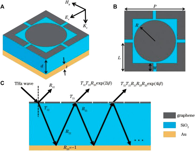
FIGURE 1. Proposed THz absorber design. (A) 3D-view; (B) top view; (C) wave propagation.
The absorber is simulated and its structural parameters are optimized through COMSOL simulation software. The absorptivity of the device
To clearly reveal the principle of terahertz absorbers, multiple reflection interference theory (MRIT) is used (Chen, 2012; Yang et al., 2020). Figure 1C shows the propagation path of THz waves in the absorber. The terahertz wave enters the absorber obliquely from the air. Part of it is reflected on the upper surface of the graphene layer with a reflection coefficient of
In the formula:
The total electrical conductivity
In the formula:
In the formula:
3 Results and discussion
Set graphene’s
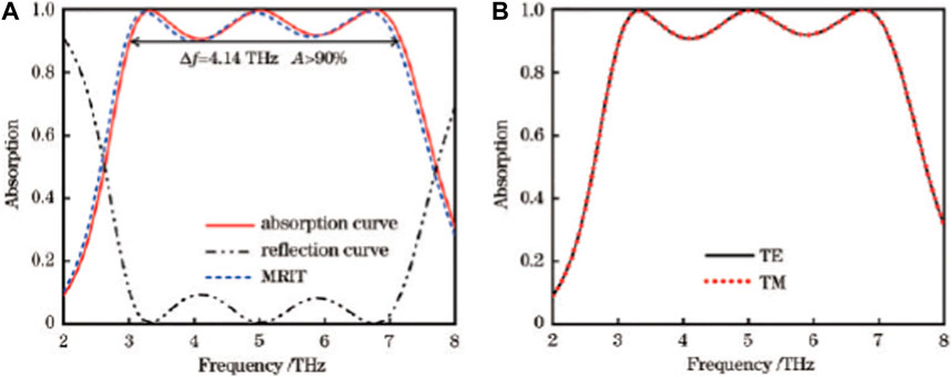
FIGURE 2. Results comparison of the proposed absorber. (A) Absorption, reflection and MRIT simulation; (B) TE and TM modes evaluation.
To explore the intrinsic procedure, the absorption spectra of graphene layers with different patterns were drawn, as shown in Figure 3A.
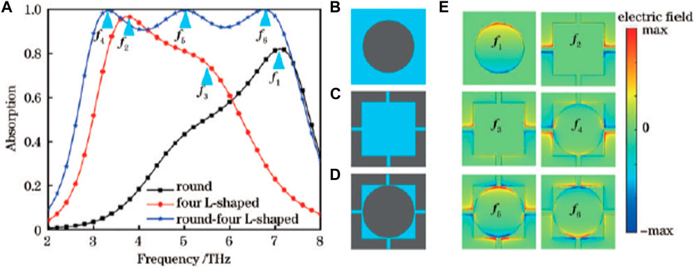
FIGURE 3. Absorption evaluation under different frequencies. (A) Absorption results of different shapes; (B) top view of circular design; (C) top view of four L-shaped design; (D) top view of circular and L-shaped design; (E) corresponding E-field in
The electric field distribution diagram (
In addition, analyzing the electric field mode distribution
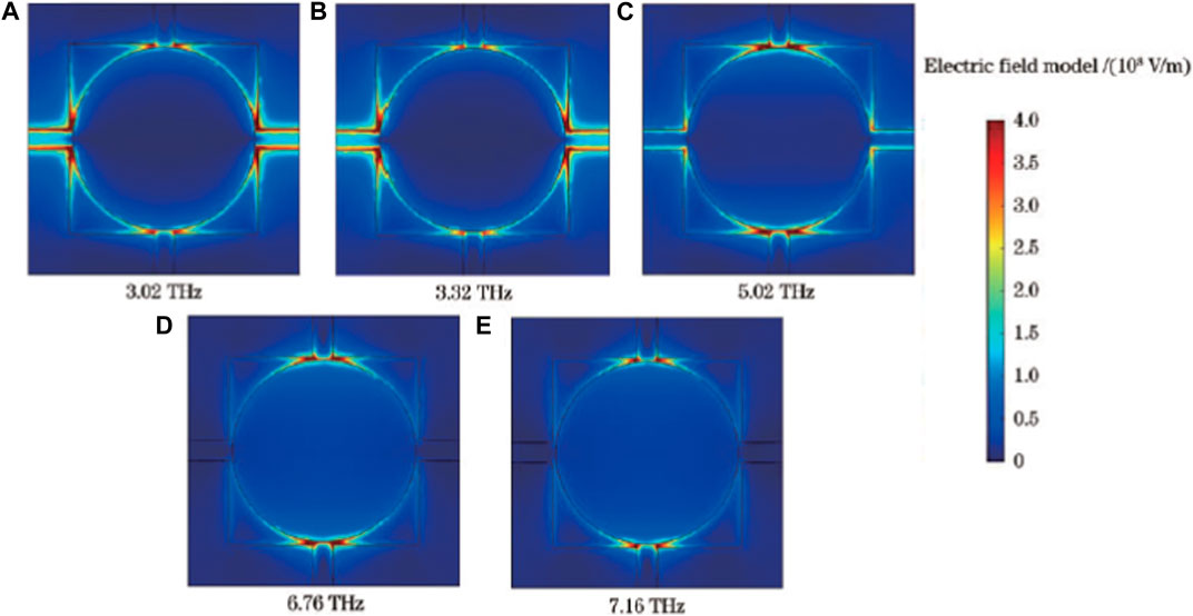
FIGURE 4. Electric field under different frequencies. (A) 3.02 THz; (B) 3.32 THz; (C) 5.02 THz; (D) 6.76 THz; (E) 7.16 THz.
The designed absorber characteristics are further characterized by changing the shape of the internal graphene. As can be seen from Figure 5A, the internal absorption of circular, regular rhombus and octagonal graphene absorbers are shown in Figures 5B–D. The circular graphene changes into regular quadrilateral and regular octagonal graphene, and it can be found that the absorption rate of the absorber does not change much (An et al., 2023; Zhang et al., 2023). The slits generated by the coupling of L-shaped and other intermediate graphene shapes always exist, and most of the electromagnetic field should be strongly localized at the slits. Therefore, a very efficient way to design ultra-broadband absorbers is to design different shapes of patterns on the top plane to construct air slits to form couplings, thereby increasing the FB and enhancing the absorption rate.
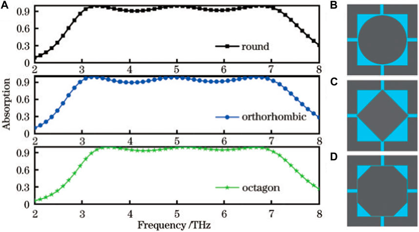
FIGURE 5. Comparison of absorption under different shapes. (A) Absorption evaluation; (B) circular; (C) quadrilateral; (D) octagonal.
By changing the parameters of the absorber structure, the magnetic permeability and dielectric constant of graphene can be adjusted (Shi et al., 2023). In order for the absorber to maintain perfect absorption, its structural parameters need to be optimized. In addition, in the actual manufacturing process, it is difficult to accurately control the geometric parameters of the device, so the impact of geometric errors on device performance will be discussed later.
As shown in Figure 6A, as the thickness of the SiO2 layer increases, the absorption curve gradually shifts to red. The absorption rate in the low-frequency part has always maintained an increasing trend. The peak at the intermediate frequency continues to maintain an absorption of more than 99%, while the high-frequency absorption peak first increases and then decreases. This is a change in SiO2 thickness that causes the absorber’s effective impedance and free space impedance to match each other at low and mid-range frequencies (Zhao et al., 2022), while matching and then breaking down at high frequencies. In Figures 6B–D, the effects of the radius
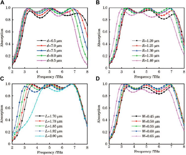
FIGURE 6. Impact of different geometrical parameters on absorption. (A) Variation with d; (B) variation with R; (C) variation with L; (D) variation with W.
During the actual use of the device, the THz wave incident from the outside is not necessarily perpendicular to the surface of the device, so it is very necessary to study the sensitivity of the polarization angle of the device. Figures 7A, B shows the absorption spectra of the device as the incident angle changes in TE and TM modes. In TE mode (Huang et al., 2023), when the incident angle changes from 0° to 70° and when it is 30°, the absorption intensity and spectrum width do not change much. As the incident angle continues to increase, the spectrum width and absorption rate slowly decrease until the incident angle is 50°, and the spectrum width with an absorption rate greater than 80% exceeds 4 THz (Lan et al., 2023). When the incident angle is greater than 50°, the absorption effect is significantly reduced, and the energy of the THz wave acting on the absorber surface is greatly reduced, so the absorption rate will decrease rapidly (Feng et al., 2021). In TM mode, when the incident angle is in the range of 0°–60°, the absorption effect and spectrum width are both very good, and when the electromagnetic wave is incident at an angle of 40°, its absorption effect is better than when it is vertically incident (Yang et al., 2023). This angle increases in TM mode, the dipoles on the surface of the absorber are effectively excited, which ultimately enhances the absorption effect. In summary, although the performance of the designed metamaterial will decrease as the incident angle increases, the designed absorber can still achieve very good absorption effects under wide-angle incidence in both polarization states.
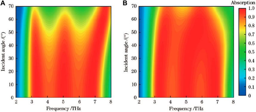
FIGURE 7. Impact of incident angle on absorption. (A) TE mode; (B) TM.
The active tunable nature of the device will have more application space in practice. Figure 8 compared the impact of different
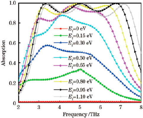
FIGURE 8. Impact of graphene fermi energy levels on absorption.
In the formula: Fermi speed
Table 1 compared the performance parameters of the proposed design with other similar absorbers. The proposed design has a simple structure and far exceeds other similar absorbers in terms of bandwidth >90% (FB) and relative bandwidth, which can be deployed in emerging applications such as energy conversion and electromagnetic shielding.
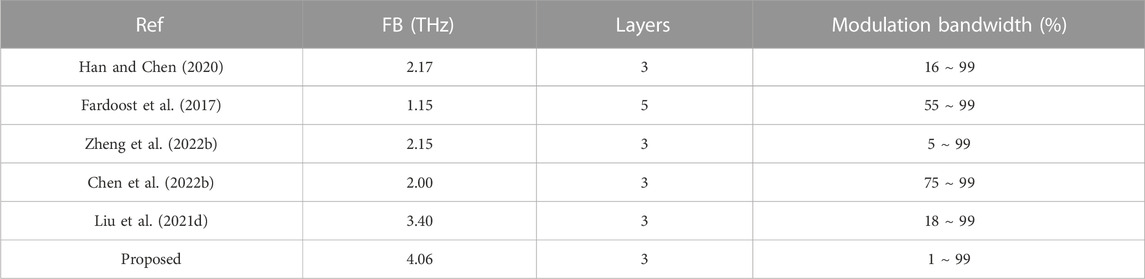
TABLE 1. Comparison of proposed and existing THz modulators.
4 Conclusion
In this article, a polarization-insensitive, functionally tunable and highly sensitive ultra-broadband absorber is designed based on graphene metamaterial. The proposed absorber dynamically alternates between ultra-wideband perfect absorption and total reflection by adjusting the applied voltage to change the Fermi level of graphene. When the Fermi level of graphene is adjusted to 0.95 eV, the absorption rate of the device is higher than 90% in the range of 3.02 ∼ 7.16 THz. Through the analysis of electromagnetic field distribution (|
Data availability statement
The original contributions presented in the study are included in the article/Supplementary material, further inquiries can be directed to the corresponding authors.
Author contributions
JT: Conceptualization, Methodology, Resources, Writing–original draft. NS: Data curation, Software, Validation, Visualization, Writing–original draft. IK: Data curation, Formal Analysis, Investigation, Supervision, Writing–review and editing. JC: Formal Analysis, Funding acquisition, Investigation, Methodology, Visualization, Writing–review and editing. HCC: Methodology, Validation, Writing, review and editing. DM: Funding acquisition, Methodology, Project administration, Resources, Supervision, Writing–original draft.
Funding
The authors would like to acknowledge the Princess Nourah bint Abdulrahman University Researchers Supporting Project number (PNURSP2023R66), Princess Nourah bint Abdulrahman University, Riyadh, Saudi Arabia. This work was supported by the National Research Foundation of Korea (NRF) grant funded by the Korean government (MSIT) (No. 2022R1C1C1004590).
Conflict of interest
The authors declare that the research was conducted in the absence of any commercial or financial relationships that could be construed as a potential conflict of interest.
Publisher’s note
All claims expressed in this article are solely those of the authors and do not necessarily represent those of their affiliated organizations, or those of the publisher, the editors and the reviewers. Any product that may be evaluated in this article, or claim that may be made by its manufacturer, is not guaranteed or endorsed by the publisher.
References
Amin, M., Siddiqui, O., Abutarboush, H., Farhat, M., and Ramzan, R. (2021). A THz graphene metasurface for polarization selective virus sensing. Carbon 176 (3), 580–591. doi:10.1016/j.carbon.2021.02.051
An, Z., Huang, Y., and Zhang, R. (2023). High-temperature multispectral stealth metastructure from the microwave-infrared compatible design. Compos. Part B Eng. 259, 110737. doi:10.1016/j.compositesb.2023.110737
Andryieuski, A., and Lavrinenko, A. (2013). Graphene metamaterials based tunable terahertz absorber: effective surface conductivity approach. Opt. Express 21 (7), 9144–9155. doi:10.1364/oe.21.009144
Bing, P., Guo, X., Wang, H., Li, Z., and Yao, J. (2019). Characteristic analysis of a photoexcited tunable metamaterial absorber for terahertz waves. J. Opt. 48, 179–183. doi:10.1007/s12596-019-00533-1
Bordbar, A., Basiry, R., and Yahaghi, A. (2020). Design and equivalent circuit model extraction of a broadband graphene metasurface absorber based on a hexagonal spider web structure in the terahertz band. Appl. Opt. 59 (7), 2165–2172. doi:10.1364/ao.385476
Cai, X., Tang, R., Zhou, H., Li, Q., Ma, S., Wang, D., et al. (2021). Dynamically controlling terahertz wavefronts with cascaded metasurfaces. Adv. Photonics 3 (3), 036003. doi:10.1117/1.ap.3.3.036003
Chen, H., Chen, Z., Yang, H., Wen, L., Yi, Z., Zhou, Z., et al. (2022b). Multi-mode surface plasmon resonance absorber based on dart-type single-layer graphene. RSC Adv. 12 (13), 7821–7829. doi:10.1039/d2ra00611a
Chen, L., Zhao, Y., Li, M., Li, L., Hou, L., and Hou, H. (2021b). Reinforced AZ91D magnesium alloy with thixomolding process facilitated dispersion of graphene nanoplatelets and enhanced interfacial interactions. Mater. Sci. Eng. A 804, 140793. doi:10.1016/j.msea.2021.140793
Chen, T. (2012). Interference theory of metamaterial perfect absorbers. Opt. Express 20 (7), 7165–7172. doi:10.1364/oe.20.007165
Chen, X., Chai, Q., Jin, M., and He, T. (2022a). Terahertz metamaterial absorbers. Adv. Mater. Technol. 7 (5), 2022, 2101171. doi:10.1002/admt.202101171
Chen, Z., Chen, H., Yin, J., Zhang, R., Jile, H., Xu, D., et al. (2021a). Multi-band, tunable, high figure of merit, high sensitivity single-layer patterned graphene: perfect absorber based on surface plasmon resonance. Diam. Relat. Mater. 116, 108393. doi:10.1016/j.diamond.2021.108393
Cheng, Y., Wang, Y., Niu, Y., and Zhao, Z. (2020). Concealed object enhancement using multi-polarization information for passive millimeter and terahertz wave security screening. Opt. Express 28 (5), 6350–6366. doi:10.1364/oe.384029
Deng, B., Guo, Q., Li, C., Wang, H., Ling, X., Farmer, D. B., et al. (2016). Coupling-Enhanced broadband mid-infrared light absorption in graphene plasmonic nanostructures. ACS Nano 10 (12), 11172–11178. doi:10.1021/acsnano.6b06203
Ding, G., Anselmi, N., Xu, W., Li, P., and Rocca, P. (2023). Interval-bounded optimal power pattern synthesis of array antenna excitations robust to mutual coupling. IEEE Antennas Wirel. Propag. Lett. 22 (11), 2725–2729. doi:10.1109/lawp.2023.3291428
Fardoost, A., Vanani, F., Amirhosseini, A., et al. (2017). Design of a multilayer graphene-based ultrawideband terahertz absorber. IEEE Trans. Nanotechnol. 16 (1), 68–74. doi:10.1109/TNANO.2016.2627939
Feng, H., Xu, Z., Li, K., Wang, M., Xie, W., Luo, Q., et al. (2021). Tunable polarization independent and angle-insensitive broadband terahertz absorber with graphene metamaterials. Opt. Express 29 (5), 7158–7167. doi:10.1364/oe.418865
Han, J., and Chen, R. (2020). Tunable broadband terahertz absorber based on a single-layer graphene metasurface. Opt. Express 28 (20), 30289–30298. doi:10.1364/oe.403631
Hossain, M., Rahman, M., and Faruque, M. (2023). An innovative polarisation-insensitive perfect metamaterial absorber with an octagonal-shaped resonator for energy harvesting at visible spectra. Nanomaterials 13 (12), 1882–1916. doi:10.3390/nano13121882
Huang, M., Wei, K., Wu, P., Xu, D., and Xu, Y. (2021). Terahertz broadband absorber based on a combined circular disc structure. Micromachines 12 (11), 1290–1310. doi:10.3390/mi12111290
Huang, X., Zhang, X., Zhou, L., Xu, J., and Mao, J. (2023). Low-loss self-packaged ka-band LTCC filter using artificial multimode SIW resonator. IEEE Trans. Circuits Syst. II Express Briefs 70 (2), 451–455. doi:10.1109/tcsii.2022.3173712
Lan, G., Tang, L., Dong, J., Nong, J., Luo, P., Li, X., et al. (2023). Enhanced asymmetric light-plasmon coupling in graphene nanoribbons for high-efficiency transmissive infrared modulation. China, Laser & Photonics Reviews.
Lan, J., Zhang, R., Bai, H., Zhang, C., Zhang, X., Hu, W., et al. (2022). Tunable broadband terahertz absorber based on laser-induced graphene. Chin. Opt. Lett. 20 (7), 073701. doi:10.3788/col202220.073701
Li, A., Masouros, C., Swindlehurst, A. L., and Yu, W. (2021b). 1-Bit massive MIMO transmission: embracing interference with symbol-level precoding. IEEE Commun. Mag. 59 (5), 121–127. doi:10.1109/mcom.001.2000601
Li, A., Masouros, C., Vucetic, B., Li, Y., and Swindlehurst, A. (2021c). Interference exploitation precoding for multi-level modulations: closed-form solutions. IEEE Trans. Commun. 69 (1), 291–308. doi:10.1109/tcomm.2020.3031616
Li, M., Guo, Q., Chen, L., Li, L., Hou, H., and Zhao, Y. (2022c). Microstructure and properties of graphene nanoplatelets reinforced AZ91D matrix composites prepared by electromagnetic stirring casting. J. Mater. Res. Technol. 21, 4138–4150. doi:10.1016/j.jmrt.2022.11.033
Li, T., Chen, H., Sun, A., Yang, X., Shangguan, Y., et al. (2022b). Microtopography-guided chessboard-like structure for a broadband terahertz absorber. ACS Appl. Electron. Mater. 4 (6), 2822–2830. doi:10.1021/acsaelm.2c00325
Li, Z., Xia, H., Zhao, Y., Lei, W., Zhao, C., and Xie, W., (2022a). Polarization-insensitive and absorption-tunable ultra-broadband terahertz metamaterial absorbers based on multiple resonant rings,” Results Phys., vol. 39, pp. 1–6. doi:10.1016/j.rinp.2022.105786
Li, Z., Yi, Z., Liu, T., Liu, L., Chen, X., Zheng, F., et al. (2021a). Three-band perfect absorber with high refractive index sensing based on an active tunable Dirac semimetal. Phys. Chem. Chem. Phys. PCCP 23 (32), 17374–17381. doi:10.1039/d1cp01375k
Liu, M., Guo, L., and Zhang, M. (2021d). Analytical method for designing tunable terahertz absorbers with the desired frequency and bandwidth. Opt. Express 29 (24), 39777–39787. doi:10.1364/oe.442425
Liu, W., Lv, Y., Tian, J., and Yang, R. (2021c). A compact metamaterial broadband THz absorber consists of graphene crosses with different sizes. Superlattices Microstruct. 159, 107038. doi:10.1016/j.spmi.2021.107038
Liu, W., Xu, J., and Song, Z. (2021a). Bifunctional terahertz modulator for beam steering and broadband absorption based on a hybrid structure of graphene and vanadium dioxide. Opt. Express 29 (15), 23331–23340. doi:10.1364/oe.433364
Liu, W., Zhang, L., Su, Q., Xu, Q., Guo, L., Yu, Z., et al. (2022). Interdigitated photoconductive antenna-based two-color femtosecond laser filamentation THz time-domain spectral detection. Opt. Express 30 (11), 18562–18570. doi:10.1364/oe.456194
Liu, Y., Huang, R., and Ouyang, Z. (2021b). Terahertz absorber with dynamically switchable dual-broadband based on a hybrid metamaterial with vanadium dioxide and graphene. Opt. Express 29 (13), 20839–20850. doi:10.1364/oe.428790
Lu, Y., Liu, W., Tian, J., and Yang, R. (2022). Broadband terahertz metamaterial absorber and modulator based on hybrid graphene-gold pattern. Phys. E Low-Dimensional Syst. Nanostructures 140, 115142. doi:10.1016/j.physe.2022.115142
Lu, Y., Stegmaier, M., Nukala, P., Giambra, M. A., Ferrari, S., Busacca, A., et al. (2017). Mixed-mode operation of hybrid phase-change nanophotonic circuits. Nano Lett. 17 (1), 150–155. doi:10.1021/acs.nanolett.6b03688
Miaofen, L., Youmin, L., Tianyang, W., Fulei, C., and Zhike, P. (2023). Adaptive synchronous demodulation transform with application to analyzing multicomponent signals for machinery fault diagnostics. Mech. Syst. Signal Process. 191, 110208. doi:10.1016/j.ymssp.2023.110208
Nie, R., He, C., Zhang, R., and Song, Z. (2023). Vanadium dioxide-based terahertz metasurfaces for manipulating wavefronts with switchable polarization. Opt. Laser Technol. 159, 109010. doi:10.1016/j.optlastec.2022.109010
Ning, J., Chen, K., Zhao, W., Zhao, J., Jiang, T., and Feng, Y. (2022). An ultrathin tunable metamaterial absorber for lower microwave band based on magnetic nanomaterial. Nanomaterials 12 (13), 2135–2214. doi:10.3390/nano12132135
Olariu, T., Beck, M., and Faist, J. (2023). Post-process frequency tuning of single-mode quantum cascade laser at 4.7 THz. IEEE J. Quantum Electron. 59 (5), 1–7. doi:10.1109/jqe.2023.3295402
Pan, Z., Zhou, Z., and Song, Z. (2023). Terahertz generations of transmissive deflection, focusing, and orbital angular momentum with polarization conversion. Opt. Laser Technol. 159, 109036. doi:10.1016/j.optlastec.2022.109036
Qian, J., Zhou, J., Zhu, Z., Ge, Z., Wu, S., Liu, X., et al. (2021). Polarization-insensitive broadband THz absorber based on circular graphene patches. Nanomaterials 11 (10), 2709–2713. doi:10.3390/nano11102709
Shen, H., Liu, F., Liu, C., Zeng, D., Guo, B., Wei, Z., et al. (2020). A polarization-insensitive and wide-angle terahertz absorber with ring-porous patterned graphene metasurface. Nanomaterials 10 (7), 1410–1411. doi:10.3390/nano10071410
Shi, J., Li, Z., Jia, J., Li, Z., Shen, C., Zhang, J., et al. (2023). Waveform-to-Waveform end-to-end learning framework in a seamless fiber-terahertz integrated communication system. J. Light. Technol. 41 (8), 2381–2392. doi:10.1109/jlt.2023.3236400
Sung, S., Dabironezare, S., Llombart, N., Brown, E., Grundfest, W. S., Taylor, Z. D., et al. (2018). Optical system design for noncontact, normal incidence, THz imaging of in vivo human cornea. IEEE Trans. Terahertz Sci. Technol. 8 (1), 1–12. doi:10.1109/tthz.2017.2771754
Wang, Q., Li, P., Rocca, P., Li, R., Tan, G., Hu, N., et al. (2023). Interval-based tolerance analysis method for petal reflector antenna with random surface and deployment errors. IEEE Trans. Antennas Propag. 71 (11), 8556–8569. doi:10.1109/tap.2023.3314097
Wu, L., Zheng, Y., Luo, Y., Zhang, J., Yi, Z., Wu, X., et al. (2021). A four-band and polarization-independent BDS-based tunable absorber with high refractive index sensitivity. Phys. Chem. Chem. Phys. PCCP 23 (47), 26864–26873. doi:10.1039/d1cp04568g
Xie, T., Chen, D., Yang, H., et al. (2021a). Tunable broadband terahertz waveband absorbers based on fractal technology. Nanomaterials 11 (2), 1–13.
Xie, T., Chen, D., Yang, H., Xu, Y., Zhange, Z., and Yang, J. (2021b). Tunable broadband terahertz waveband absorbers based on fractal technology of graphene metamaterial. Nanomaterials 11 (2), 269–313. doi:10.3390/nano11020269
Xu, B., Gu, Q., Li, Z., and Niu, Z. y. (2013). A novel structure for tunable terahertz absorber based on graphene. Opt. Express 21 (20), 23803–23811. doi:10.1364/oe.21.023803
Xu, K., Guo, Y., Liu, Y., Deng, X., Chen, Q., and Ma, Z. (2021). 60-GHz compact dual-mode on-chip bandpass filter using GaAs technology. IEEE Electron Device Lett. 42 (8), 1120–1123. doi:10.1109/led.2021.3091277
Yang, D., Zhang, C., Ju, X., Ji, Y., and Lan, C. (2020). Multi-resonance and ultra-wideband terahertz metasurface absorber based on micro-template-assisted self-assembly method. Opt. Express 28 (2), 2547–2556. doi:10.1364/oe.381927
Yang, M., Cai, C., Wang, D., Wu, Q., Liu, Z., and Wang, Y. (2023). Symmetric differential demodulation-based heterodyne laser interferometry used for wide frequency-band vibration calibration. IEEE Trans. Industrial Electron., 1–9. doi:10.1109/TIE.2023.3299015
Yao, H., Sun, Z., Liang, L., Yan, X., Wang, Y., Yang, M., et al. (2023). Hybrid metasurface using graphene/graphitic carbon nitride heterojunctions for ultrasensitive terahertz biosensors with tunable energy band structure. Photonic Res. 11 (5), 858–868. doi:10.1364/prj.482256
Yin, X., Wadji, A., and Zhang, Y. (2022). A biomedical perspective in terahertz nano-communications: a review. IEEE Sensors J. 22 (10), 9215–9227. doi:10.1109/jsen.2022.3161013
Zhang, M., and Song, Z. (2021). Switchable terahertz metamaterial absorber with broadband absorption and multiband absorption. Opt. Express 29 (14), 21551–21561. doi:10.1364/oe.432967
Zhang, Q., Xu, Q., Xia, L., Li, Y., Gu, J., Tian, Z., et al. (2020). Terahertz surface plasmonic waves: a review. Adv. Photonics 2 (1), 014001. doi:10.1117/1.ap.2.1.014001
Zhang, R., Luo, Y., Xu, J., Wang, H., Han, H., Hu, D., et al. (2021a). Structured vanadium dioxide metamaterial for tunable broadband terahertz absorption. Opt. Express 29 (26), 42989–42998. doi:10.1364/oe.447949
Zhang, Y., He, Y., Wang, H., Sun, L., and Su, Y. (2021b). Ultra-broadband mode size converter using on-chip metamaterial-based luneburg lens. ACS Photonics 8 (1), 202–208. doi:10.1021/acsphotonics.0c01269
Zhang, Y., Zhao, P., Lu, Q., Zhang, Y., Lei, H., Yu, C., et al. (2023). Functional additive manufacturing of large-size metastructure with efficient electromagnetic absorption and mechanical adaptation. Compos. Part A Appl. Sci. Manuf. 173, 107652. doi:10.1016/j.compositesa.2023.107652
Zhao, J., Zhou, M., Chen, J., Wang, L., Zhang, Q., Zhong, S., et al. (2023). Two birds one stone: graphene assisted reaction kinetics and ionic conductivity in phthalocyanine-based covalent organic framework anodes for lithium-ion batteries. Nano-Micro Small 19 (44), 2303353. doi:10.1002/smll.202303353
Zhao, Z., Xu, G., Zhang, N., and Zhang, Q. (2022). Performance analysis of the hybrid satellite-terrestrial relay network with opportunistic scheduling over generalized fading channels. IEEE Trans. Veh. Technol. 71 (3), 2914–2924. doi:10.1109/tvt.2021.3139885
Zheng, L., Feng, R., Shi, H., and Li, X. (2023). Tunable broadband terahertz metamaterial absorber based on vanadium dioxide and graphene. Micromachines 14 (9), 1715–1812. doi:10.3390/mi14091715
Zheng, P., Luo, Y., Yang, H., Yi, Z., Zhang, J., Song, Q., et al. (2022b). Thermal tuning of terahertz metamaterial absorber properties based on VO2. Phys. Chem. Chem. Phys. PCCP 24 (15), 8846–8853. doi:10.1039/d2cp01070d
Zheng, P., Zheng, Y., Luo, Y., Yi, Z., Zhang, J., Liu, L., et al. (2021). Terahertz perfect absorber based on flexible active switching of ultra-broadband and ultra-narrowband. Opt. Express 29 (26), 42787–42799. doi:10.1364/oe.445155
Zheng, P., Zheng, Y., Luo, Y., Yi, Z., Zhang, J., Liu, Z., et al. (2022a). A switchable terahertz device combining ultra-wideband absorption and ultra-wideband complete reflection. Phys. Chem. Chem. Phys. PCCP 24 (4), 2527–2533. doi:10.1039/d1cp04974g
Zhou, Z., and Song, Z. (2022). Terahertz mode switching of spin reflection and vortex beams based on graphene metasurfaces. Opt. Laser Technol. 153, 2022, 108278. doi:10.1016/j.optlastec.2022.108278
Zhu, J., Wu, C., and Ren, Y., (2021). Broadband terahertz metamaterial absorber based on graphene resonators with perfect absorption,” Results Phys., vol. 26, pp. 1–7. doi:10.1016/j.rinp.2021.104466
Keywords: graphene, THz modulator, nanotechnology, computational optimization, absorber
Citation: Tiang JJ, Soliman NF, Khan I, Choi J, Chung HC and Madsen DØ (2023) Design and performance evaluation of a novel broadband THz modulator based on graphene metamaterial for emerging applications. Front. Mater. 10:1305793. doi: 10.3389/fmats.2023.1305793
Received: 02 October 2023; Accepted: 08 November 2023;
Published: 21 November 2023.
Edited by:
Giuseppe Failla, Mediterranea University of Reggio Calabria, ItalyReviewed by:
Zhengyong Song, Xiamen University, ChinaErkan Danaci, TUBITAK National Metrology Institute (NMI), Türkiye
Copyright © 2023 Tiang, Soliman, Khan, Choi, Chung and Madsen. This is an open-access article distributed under the terms of the Creative Commons Attribution License (CC BY). The use, distribution or reproduction in other forums is permitted, provided the original author(s) and the copyright owner(s) are credited and that the original publication in this journal is cited, in accordance with accepted academic practice. No use, distribution or reproduction is permitted which does not comply with these terms.
*Correspondence: Jaeyoung Choi, anljaG9pMTlAZ2FjaG9uLmFjLmty; Dag Øivind Madsen, ZGFnLm9pdmluZC5tYWRzZW5AdXNuLm5v