 Jinggao Sui
 Xiang Lan2†
 Baihui Zhang
 Mianzeng Zhong
 Jinhui Cao
- 1Defense Innovation Institute, Academy of Military Sciences, Beijing, China
- 2School of Materials Science and Engineering, Hunan University, Changsha, China
- 3Hunan Key Laboratory of Nanophotonics and Devices, School of Physics, Central South University, Changsha, China
- 4Department of Physics, College of Sciences, National University of Defense Technology, Changsha, China
- 5College of Energy and Power Engineering, Changsha University of Science and Technology, Changsha, China
Low-dimensional nanomaterials have garnered significant interest for their unique electronic and optical properties, which are essential for advancing next-generation optoelectronic devices. Among these, tellurium suboxide (TeOx)-based nanowires (NWs), with their quasi-one-dimensional (1D) structure, offer distinct advantages in terms of charge transport and light absorption. In this study, we present a comprehensive investigation into the controlled synthesis, structural properties, and optoelectronic performance of TeOx nanowires. Nanowires were synthesized via chemical vapor deposition process and exhibited a high aspect ratio with excellent structural quality, confirmed through Raman spectroscopy, scanning electron microscopy (SEM), and transmission electron microscopy (TEM). The TeOx nanowires demonstrated high crystallinity, smooth surface morphology, and consistent growth across the substrate, making them suitable for scalable device fabrication. The optoelectronic characterization of a fabricated photodetector, based on a single TeOx nanowire, revealed remarkable photoresponsivity and stability across a broad range of light intensities. These findings position TeOx nanowires as promising candidates for future optoelectronic devices such as photodetectors and optical sensors.
1 Introduction
The development of advanced photodetectors is critical for a broad range of applications, including imaging, sensing, environmental monitoring and communication systems (Wang et al., 2019; Yao and Yang, 2020). Despite significant progress in recent years, conventional photodetectors often suffer from several limitations, such as restricted responsivity, slow response times, limited detection range and sophisticated fabrication techniques (Jiang et al., 2020). These drawbacks restrict the utility of traditional photodetection systems in demanding applications. For instance, silicon-based photodetectors, though widely used, are typically limited by their narrow spectral range and vulnerability to environmental factors such as high humidity and extreme temperatures, leading to performance degradation over time (Goossens et al., 2021; Liu et al., 2021).
In contrast, low-dimensional nanomaterials have garnered substantial attention due to their distinctive electronic and optical properties, which are critical for advancing next-generation optoelectronic devices. Among these, one-dimensional (1D) nanostructures exhibit unique characteristics such as high aspect ratio and anisotropic carrier transport (Wei et al., 2023), making them highly attractive for various applications in photodetection (An et al., 2018; Li et al., 2023; Wei et al., 2024), sensing (Zhao et al., 2014; Zafar et al., 2018) and energy storage (Zhou et al., 2019; Nehra et al., 2020; Jin et al., 2023). In particular, TeOx-based nanowires (NWs), with their quasi-1D morphology, provide significant advantages in terms of charge transport (Liu et al., 2008) and photoresponse (Zhang et al., 2023), positioning them as promising candidates for high-performance optoelectronic devices.
As a p-type semiconductor, TeOx exhibits a favorable band alignment for efficient charge separation in optoelectronic devices (Zhou et al., 2020). The reduced surface recombination effects and enhanced carrier mobility within the nanowires contribute to their superior photodetection capabilities (Koo and Kim, 2009; Wu et al., 2014). These features, combined with their scalability and compatibility with existing semiconductor technologies, position TeOx NWs as versatile building blocks for integrated photonic devices.
In this study, we present a systematic approach to the controlled growth of TeOx nanowires and provides insights into their optoelectronic performance. By fine-tuning the oxidation line and growth parameters, we achieve TeOx nanowires with high aspect ratios and excellent optoelectronic properties. Raman spectrum, scanning electron microscopy (SEM) and transmission electron microscopy (TEM) present the excellent crystal structure of as-prepared TeOx nanowires. Optoelectronic characterization demonstrates that TeOx-based photodetectors hold significant promise for applications requiring broad-spectrum light detection and high responsivity, paving the way for their use in next-generation optoelectronic and photonic systems.
2 Experimental details
2.1 Synthesis of TeOx nanowires
As shown in Figure 1A, a quartz boat containing Te powder (∼10 g) is located in the central heating zone of the furnace, and a clean silicon dioxide (∼275 nm)/Si substrate is located at the end of the furnace as the growth substrate. The horizontal distance between the powder and the silicon wafer should be kept between 10 cm. During the process of temperature increase, place the growth substrate upstream of the source and set the airflow to 300 sccm (along the black arrow in Figure 1A) for 15 min to remove unwanted water vapor. Then maintain the Ar gas flow at 120 sccm. When the central heating zone reaches the target temperature of 400°C, maintain it for 10 min for growth. Next, stop heating and let it cool naturally to room temperature. The entire process is carried out under ambient pressure in an argon/O2 atmosphere.

Figure 1. Synthesis Strategy of TeOx nanowires. (A) Schematic diagram of the synthesis device for synthesizing TeOx nanowires. (B, C) Chemical vapor deposition process of TeOx nanowires. TeOx nanowires are synthesized on a substrate by the reaction of Te source and oxygen.
2.2 Characterization
SEM and TEM are used to characterize the morphology of TeOx nanowires. Raman spectroscopy analysis was performed using a Renishaw confocal Raman system excited by a 488 nm laser at room temperature. The applied laser power is set to 5%, and the exposure time is approximately 0.1 s Preparation of TEM samples using polymethyl methacrylate (PMMA) assisted method. Spin coat PMMA onto the heterojunction sample until the PMMA layer completely covers the heterojunction sample, then bake at 180°C for 3 min. Afterwards, immerse the wafer in a saturated 0.2 M NaOH solution to, etch the SiO2 layer. After separating the PMMA coated sample from the silicon wafer, it was repeatedly transferred to fresh deionized water to wash away residual contaminants, and then captured using a traditional Lacey carbon film TEM grid. The transferred sample is naturally dried in the surrounding environment and then immersed in acetone overnight to clean the PMMA coating. All TEM samples were baked at 100°C for 10 min.
3 Results and discussion
3.1 Structural and morphological characterization of TeOx nanowires
Here, we demonstrate the feasibility of thermodynamic control of chemical reactions for synthesizing TeOx nanowires of different sizes. The synthesis strategy is depicted in Figure 1B, C. In our experiment, we successfully grew TeOx nanowires (Figure 2A). By adjusting the reaction temperature, two distinct growth trends were observed. When the growth temperature is low, the reaction between Te and O2 tends to grow into nanorods with relatively small aspect ratios (Figure 2B). When the growth temperature is high, the morphology of TeOx nanowires tends to have a high aspect ratio, as shown in Figure 2C. This can be attributed to the relatively weak evaporation ability of Te at 260°C, resulting in a lower nucleation density.

Figure 2. CVD growth for TeOx nanowires. (A) Typical optical micrograph of the TeOx NWs. Scale bar, 200 μm. (B) Optical image of TeOx nanowires grown at 260°C. Scale bar, 50 μm. (C) Optical image of TeOx nanowires grown at 460°C. Scale bar, 50 μm.
The structural properties of the synthesized TeOx nanowires were characterized using a combination of Raman spectroscopy, scanning electron microscopy, transmission electron microscopy, and selected area electron diffraction (SAED). These techniques provided comprehensive insights into the crystallinity and morphological features of the nanowires, confirming their high structural quality.
As shown in Figure 3A, the Raman spectrum of TeOx nanowires exhibit prominent peaks at A1 and E2 modes, indicating the well-ordered crystalline structure of TeOx. The peak at approximately 267.7 cm−1 in B2 mode is assigned to the characteristic vibrational modes of the Te-O bond (Yan and Kang, 2014), reflecting the formation of the TeOx phase. The sharpness of the Raman peaks further confirms the high crystallinity of the nanowires, which is crucial for their enhanced optoelectronic properties (Liao et al., 2014). High crystallinity typically reduces the defects and grain boundaries, allowing for the efficient charge carrier transport (Wang et al., 2022). This characteristic is especially critical in optoelectronic devices, where any disruption in the lattice structure can lead to scattering and recombination of charge carriers, thereby reducing performance.
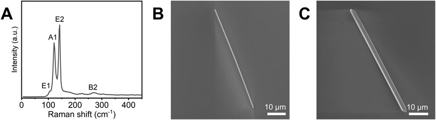
Figure 3. Morphological characterization of TeOx NWs. (A) Raman spectra of TeOx Nanowires. (B) SEM image of TeOx nanowires. (C) Magnified SEM image of TeOx NWs. Scale bar, 10 μm.
The SEM images in Figures 3B,C demonstrate the uniformity and smooth surface morphology of the synthesized TeOx nanowires. These images display a highly uniform and smooth surface morphology, which is essential for minimizing surface defects that could impede charge carrier mobility in optoelectronic applications. The nanowires exhibit a high aspect ratio, with diameters on the order of 2 μm and lengths extending up to several tens of micrometers. This high aspect ratio is particularly beneficial in enhancing the photodetection area, allowing for greater interaction with incident light, thereby improving the device’s overall sensitivity (da Silva et al., 2023). Moreover, uniformity and surface smoothness of the nanowires stated from the SEM images is important for minimizing scattering of charge carriers. The consistency in growth across the substrate is a promising sign for scalable device fabrication, ensuring repeatable performance across multiple devices. At lower growth temperatures (∼260°C), incomplete oxidation and insufficient thermal energy may result in poorly crystallized TeOx nanowires, leading to higher defect densities, which act as recombination centers for charge carriers. This degrades the nanowire’s electrical conductivity and reduces the photocurrent generation in photodetector applications. Furthermore, higher defect concentrations can negatively affect carrier mobility, thereby limiting the device’s response speed and sensitivity. In contrast, higher growth temperatures (∼460°C) typically promote more uniform oxidation and improved crystal quality, resulting in fewer structural defects and enhanced carrier mobility. As a result, nanowires synthesized at optimized temperatures exhibit better charge separation and transport properties, which are essential for achieving high responsivity in photodetectors. Improved crystal quality also minimizes the probability of surface recombination, enhancing the photodetector’s stability and performance over time.
Further confirm the crystal structure of TeOx nanowires using transmission electron microscopy (TEM). Low-magnification TEM images of TeOx nanowires (Figure 4A) and the corresponding high-resolution TEM images (Figure 4B) further elucidate the atomic arrangement of the TeOx nanowires. The bright spots correspond to tellurium atoms, which are distinguishable due to their high atomic number (Z = 52), while oxygen atoms have a lower atomic number (Z = 8), making them almost indistinguishable (Yamashita et al., 2018). The lattice spacing measured from the HRTEM image is approximately 0.205 nm, corresponding to the (003) planes of the TeOx crystal, indicating a high degree of crystallinity in the nanowires. Additionally, the SAED pattern (Figure 4C) shows well-defined diffraction spots, which can be indexed to the (003) planes of the TeOx phase. This confirms the single-crystalline nature of the nanowires and the preferred orientation along the [0001] direction. The diffraction pattern is consistent with the HRTEM findings, corroborating the high-quality crystal structure of the synthesized TeOx nanowires.
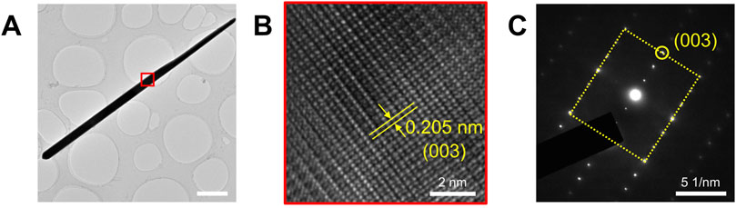
Figure 4. Structural characterization of TeOx NWs. (A) Low-magnification TEM image of TeOx NWs. Scale bar, 2 μm. (B) High-resolution TEM image selected from the red plane in (A). Scale bar, 2 nm. (C) Corresponding selected area electron diffraction patterns. Scale bar, 5 1/nm.
3.2 Optoelectronic performance of TeOx nanowire photodetector
To investigate the optoelectronic properties of the TeOx nanowires, a photodetector device was fabricated, as depicted in Figure 5A. The device was constructed by positioning a single TeOx nanowire between two gold electrodes on a SiO2/Si substrate. The Au electrodes were deposited using standard photolithography and electron beam evaporation techniques. This setup enabled the characterization of the nanowire’s photodetection capabilities under varying light intensities. The optical image provides a clear view of the fabricated device, where the TeOx nanowire is well-aligned between the gold electrodes, as shown in Figure 5B. The uniformity of the nanowire ensures consistent charge transport properties across the device, which is essential for reliable photodetection. The time-dependent photocurrent response of the device, measured under different light intensities, is shown in Figure 5C. The photocurrent increases as the light intensity increases, demonstrating the high sensitivity of the TeOx nanowire to incident light. The distinct photocurrent steps correspond to light power density ranging from 0.0015 mW/mm2 to 1.08 mW/mm2, indicating the device’s ability to detect light over a wide intensity range. This behavior suggests that the TeOx nanowire photodetector exhibits a rapid and repeatable response to light, making it highly suitable for optoelectronic applications such as photodetectors and optical sensors. The device shows stable switching behavior, with well-defined on/off states in the photocurrent response. This stability is indicative of low trap-state density in the nanowires and the high quality of the material. The high photocurrent under illumination, combined with the quick recovery to baseline in the absence of light, underscores the potential of TeOx nanowires for use in high-performance, low-power photodetectors. By the rational device design and high-quality material preparation, TeOx nanowires are expected to play an important role in future optoelectronic applications (Zhang et al., 2024).

Figure 5. Optoelectronic performance of TeOx NWs. (A) Schematic illustration of the TeOx nanowire photodetection device. (B) Optical image of the photodetector device. Scale bar, 5 μm. (C) Time-resolved photocurrent response of the devices under light power densities from 0.0015 to 1.08 mW/mm2 with the wavelength of 638 nm.
4 Conclusion
In this study, we successfully synthesized TeOx nanowires with high structural quality using a thermal oxidation method, and systematically characterized their morphological and optoelectronic properties. Raman spectroscopy confirmed the well-ordered crystalline structure of the nanowires, while SEM and TEM analyses revealed their smooth surface morphology and high aspect ratio, critical for enhancing charge transport and light absorption. The photodetector fabricated using a single TeOx nanowire exhibited high sensitivity, stable on/off switching behavior, and rapid photocurrent response to varying light intensities. These results highlight the potential of TeOx nanowires for use in high-performance, low-power optoelectronic devices. Given the excellent material quality and device performance, TeOx nanowires are poised to become key building blocks for next-generation photodetectors and integrated photonic systems.
Data availability statement
The original contributions presented in the study are included in the article/supplementary material, further inquiries can be directed to the corresponding authors.
Author contributions
JS: Supervision, Methodology, Writing–original draft. XL: Data curation, Formal Analysis, Writing–review and editing. BZ: Writing–review and editing, Validation. MZ: Writing–review and editing, Conceptualization. GW: Conceptualization, Writing–review and editing. JC: Conceptualization, Writing–review and editing, Supervision.
Funding
The author(s) declare that no financial support was received for the research, authorship, and/or publication of this article.
Conflict of interest
The authors declare that the research was conducted in the absence of any commercial or financial relationships that could be construed as a potential conflict of interest.
The reviewer DL declared a shared affiliation with the author XL at the time of review.
Publisher’s note
All claims expressed in this article are solely those of the authors and do not necessarily represent those of their affiliated organizations, or those of the publisher, the editors and the reviewers. Any product that may be evaluated in this article, or claim that may be made by its manufacturer, is not guaranteed or endorsed by the publisher.
References
An, Q., Liu, Y., Jiang, R., and Meng, X. (2018). Chemical vapor deposition growth of ReS2 nanowires for high-performance nanostructured photodetector. Nanoscale 10, 14976–14983. doi:10.1039/c8nr04143a
Da Silva, B. C., Biegański, A., Durand, C., Sadre Momtaz, Z., Harikumar, A., Cooper, D., et al. (2023). High-aspect-ratio GaN p–i–n nanowires for linear UV photodetectors. ACS Appl. Nano Mater. 6, 12784–12791. doi:10.1021/acsanm.3c01495
Goossens, S., Konstantatos, G., and Oikonomou, A. (2021). Colloidal quantum dot image sensors: technology and marketplace opportunities. Inf. Disp. 37, 18–23. doi:10.1002/msid.1257
Jiang, Y., Karpf, S., and Jalali, B. (2020). Time-stretch LiDAR as a spectrally scanned time-of-flight ranging camera. Nat. Photonics 14, 14–18. doi:10.1038/s41566-019-0548-6
Jin, M., Teng, M., Wang, S., Yang, K., Wang, J., and Jin, H. (2023). Interface engineering of crystalline/amorphous Pt/TeOx nanocapsules for efficient alkaline hydrogen evolution. Int. J. Hydrogen Energy 48, 16593–16600. doi:10.1016/j.ijhydene.2023.01.178
Koo, J., and Kim, S. (2009). Charge transport modulation of silicon nanowire by O2 plasma. Solid State Sci. 11, 1870–1874. doi:10.1016/j.solidstatesciences.2009.08.004
Li, Y., Wang, S., Hong, J., Zhang, N., Wei, X., Zhu, T., et al. (2023). Polarization-Sensitive photodetector based on high crystallinity quasi-1D BiSeI nanowires synthesized via chemical vapor deposition. Small 19, 2302623. doi:10.1002/smll.202302623
Liao, C.-H., Huang, C.-W., Chen, J.-Y., Chiu, C.-H., Tsai, T., Lu, K.-C., et al. (2014). Optoelectronic properties of single-crystalline Zn2GeO4 nanowires. J. Phys. Chem. C 118, 8194–8199. doi:10.1021/jp500830x
Liu, J., Gao, M., Kim, J., Zhou, Z., Chung, D. S., Yin, H., et al. (2021). Challenges and recent advances in photodiodes-based organic photodetectors. Mater. Today 51, 475–503. doi:10.1016/j.mattod.2021.08.004
Liu, Z., Yamazaki, T., Shen, Y., Kikuta, T., and Nakatani, N. (2008). Synthesis and characterization of TeO2 nanowires. Jpn. J. Appl. Phys. 47, 771. doi:10.1143/jjap.47.771
Nehra, M., Dilbaghi, N., Marrazza, G., Kaushik, A., Abolhassani, R., Mishra, Y. K., et al. (2020). 1D semiconductor nanowires for energy conversion, harvesting and storage applications. Nano Energy 76, 104991. doi:10.1016/j.nanoen.2020.104991
Wang, P., Xia, H., Li, Q., Wang, F., Zhang, L., Li, T., et al. (2019). Sensing infrared photons at room temperature: from bulk materials to atomic layers. Small 15, 1904396. doi:10.1002/smll.201904396
Wang, S.-L., Frisch, S., Zhang, H., Yildiz, O., Mandal, M., Ugur, N., et al. (2022). Grain engineering for improved charge carrier transport in two-dimensional lead-free perovskite field-effect transistors. Mater. Horiz. 9, 2633–2643. doi:10.1039/d2mh00632d
Wei, B., Zou, B., Liu, J., Wang, W., Wang, W., Cao, Z., et al. (2024). Polarization-Sensitive photodetector based on quasi-1D (TaSe4)2I nanowire response to 10.6 µm. Adv. Funct. Mater. 34, 2315194. doi:10.1002/adfm.202315194
Wei, X., Wang, S., Zhang, N., Li, Y., Tang, Y., Jing, H., et al. (2023). Single-orientation epitaxy of quasi-1D tellurium nanowires on M-plane sapphire for highly uniform polarization sensitive short-wave infrared photodetection. Adv. Funct. Mater. 33, 2300141. doi:10.1002/adfm.202300141
Wu, J., Yin, B., Wu, F., Myung, Y., and Banerjee, P. (2014). Charge transport in single CuO nanowires. Appl. Phys. Lett. 105, 183506. doi:10.1063/1.4900966
Yamashita, S., Kikkawa, J., Yanagisawa, K., Nagai, T., Ishizuka, K., and Kimoto, K. (2018). Atomic number dependence of Z contrast in scanning transmission electron microscopy. Sci. Rep. 8, 12325. doi:10.1038/s41598-018-30941-5
Yan, C. Z., and Kang, D. J. (2014). Synthesis of TeO2 nanowires via a facile thermal oxidation method. Cryst. Res. Technol. 49, 400–404. doi:10.1002/crat.201400050
Yao, J., and Yang, G. (2020). 2D material broadband photodetectors. Nanoscale 12, 454–476. doi:10.1039/c9nr09070c
Zafar, S., D’emic, C., Jagtiani, A., Kratschmer, E., Miao, X., Zhu, Y., et al. (2018). Silicon nanowire field effect transistor sensors with minimal sensor-to-sensor variations and enhanced sensing characteristics. ACS Nano 12, 6577–6587. doi:10.1021/acsnano.8b01339
Zhang, B., Ao, Z., Zhang, F., Zhong, J., Zhang, S., Liu, H., et al. (2024). Controlled growth of asymmetric chiral TeOx for broad-spectrum, high-responsivity and polarization-sensitive photodetection. J. Chem. Phys. 161, 084705. doi:10.1063/5.0222227
Zhang, F., Mo, Z., Cui, B., Liu, S., Xia, Q., Li, B., et al. (2023). Bandgap engineering of BiIns nanowire for wide-spectrum, high-responsivity, and polarimetric-sensitive detection. Adv. Funct. Mater. 33, 2306077. doi:10.1002/adfm.202306077
Zhao, X., Cai, B., Tang, Q., Tong, Y., and Liu, Y. (2014). One-dimensional nanostructure field-effect sensors for gas detection. Sensors 14, 13999–14020. doi:10.3390/s140813999
Zhou, B.-X., Ding, S.-S., Wang, Y., Wang, X.-R., Huang, W.-Q., Li, K., et al. (2020). Type-II/type-II band alignment to boost spatial charge separation: a case study of g-C3N4 quantum dots/a-TiO2/r-TiO2 for highly efficient photocatalytic hydrogen and oxygen evolution. Nanoscale 12, 6037–6046. doi:10.1039/d0nr00176g
Keywords: chemical vapor deposition, tellurium, nanowires, optoelectronics, photodetectors
Citation: Sui J, Lan X, Zhang B, Zhong M, Wang G and Cao J (2024) High-performance optoelectronic devices based on TeOx nanowires: synthesis, characterization and photodetection. Front. Mater. 11:1497540. doi: 10.3389/fmats.2024.1497540
Received: 17 September 2024; Accepted: 28 October 2024;
Published: 07 November 2024.
Edited by:
Huifang Ma, Nanjing University of Posts and Telecommunications, ChinaReviewed by:
Lakshmi Narayanan Mosur Saravana Murthy, Intel, United StatesDong Li, Hunan University, China
Lili Zhang, Lanzhou University, China
Copyright © 2024 Sui, Lan, Zhang, Zhong, Wang and Cao. This is an open-access article distributed under the terms of the Creative Commons Attribution License (CC BY). The use, distribution or reproduction in other forums is permitted, provided the original author(s) and the copyright owner(s) are credited and that the original publication in this journal is cited, in accordance with accepted academic practice. No use, distribution or reproduction is permitted which does not comply with these terms.
*Correspondence: Mianzeng Zhong, em16aG9uZ0Bjc3UuZWR1LmNu; Guang Wang, d2FuZ2d1YW5nQG51ZHQuZWR1LmNu; Jinhui Cao, Y2FvamluaHVpQGhudS5lZHUuY24=
†These authors have contributed equally to this work and share first authorship