 Wei-Sung Weng1
 Lung-Chien Chen
- 1Department of Avionics, China University of Science and Technology, Taipei, Taiwan
- 2Department of Electro-Optical Engineering, National Taipei University of Technology, Taipei, Taiwan
- 3Department of Mechanical Engineering, National Taipei University of Technology, Taipei, Taiwan
In this study, we prepared MASnI3 lead (Pb)-free halide perovskite metal-semiconductor-metal-type photodetectors through the inversion crystallization method under an atmospheric environment and the spin-coating method in a glove box, respectively. The scanning electron microscopy (SEM) images revealed the different surface morphology. They show two types of growth models: the inverse temperature crystallization (ITC) method uses solvent volatilization, and the spin-coating method is a reaction between precursors. For the MASnI3 perovskite film obtained through the inversion crystallization method, a broad band of photoluminescence (PL) spectrum at approximately 470 nm, corresponding to the level transition of 2.638 eV, was observed. On the other hand, for the MASnI3 perovskite film obtained through the spin-coating method, a narrow band of the photoluminescence spectrum at approximately 773 nm, corresponding to the level transition of 1.604 eV, was observed. This is the Burstein–Moss shift environment due to the introduction of oxygen. In addition, the photocurrent of a device prepared in a glove box is two orders of magnitude higher than that of the device prepared by the ITC method.
1 Introduction
In the early part of this decade, the halide perovskite materials, like MAPbBr3, were mostly lead (Pb)-containing halide perovskites. Except for the outstanding optoelectronic properties, including high charge carrier mobility, defect tolerance, and high absorption, the characteristics regarding pinhole formation and crystallinity of perovskite materials are suitable for the application of gas sensors (Kassa et al., 2025; Lee et al., 2025; Zhai et al., 2024). However, lead-containing materials in many other related products have been proven to gradually decompose over time, making it easy to be exposed to excessive lead during use. In subsequent research on halide perovskites, it was confirmed that the lead in halide perovskites is easily soluble in water after oxidation over time, thereby polluting the environment (Wan et al., 2021). This has played an important role in promoting the research and development of lead-free halide perovskites. Among them, both tin (Sn) and lead belong to the same group of elements and have similar chemical properties, and their close covalent radii have a greater impact on the structural stability of halide perovskites. MASnI3 is an interesting material due to its very easy oxidation and degradation in ambient air. Therefore, only a few studies have compared Pb-based perovskite materials and MASnI3. The pollution caused by oxides is much less harmful than lead, making tin a popular choice to replace lead as lead-free halide perovskites, and has generated a large amount of related research (Hao et al., 2015; Noel et al., 2014; Hao et al., 2014; Stoumpos et al., 2013; Chen et al., 2016). However, tin in ABX3 halide perovskite easily transforms from Sn2+ to Sn4+, thereby destroying the stability of the structure of perovskite materials (Mitzi and Liang, 1997; Sabba et al., 2015; Yuan et al., 2022; Peng and Xie, 2020; Bouich et al., 2022; Aldamasy et al., 2021; Saha et al., 2024). Therefore, a key problem that must be solved is that these devices must overcome the degradation in the ambient environment to be profitable. This study used the halide perovskite MASnI3 as a photodetector material. In this work, we carried out the device process by the inverse temperature crystallization (ITC) method under a normal atmospheric environment to make an MASnI3 halide perovskite film on the glass substrates with an ITO electrode pattern and observed their surface images with SEM. The image of the film growth crystal and the I-V characteristics were investigated using a photocurrent induced by different wavelengths of visible light and infrared. In addition, we prepared the MASnI3 perovskite film deposited by the spin-coating method to compare the different characteristics of films obtained by the ITC and spin coating methods.
2 Materials and methods
First, the MAI (0.11 g) and SnI2 (0.27 g), respectively, were put in a glass beaker, and then a pipette was used to add 0.5 mL of γ-butyrolactone (GBL) solution into the glass beaker, which was stirred with a magnet that was cleaned using ethanol and blown dry with nitrogen. The beaker was sealed with tape and placed on an electromagnetic heating stirrer to stir at 500 rpm for 24 h to form a 1.5 M MASnI3 precursor solution, as shown in Figure 1a (Yuan et al., 2022; Peng and Xie, 2020). Next, the ITO glass was cleaned with an ultrasonic oscillator using organic acetone or IPA solution for 5 min. It was placed in an ultraviolet lighting machine for 10 min to form a hydrophilic surface. Then, the MASnI3 precursor solution was dropped onto the surface of the ITO glass substrate and moved into an oven for baking at 100°C for approximately 5–7 days to form the MASnI3 film, as shown in Figures 1b,c. For the second sample, we prepared the MASnI3 perovskite film metal-semiconductor-metal-type photodetector on the glass substrate with an ITO pattern deposited by the spin-coating method (3,000 rpm) using the same precursor solution, as shown in Figure 1d.
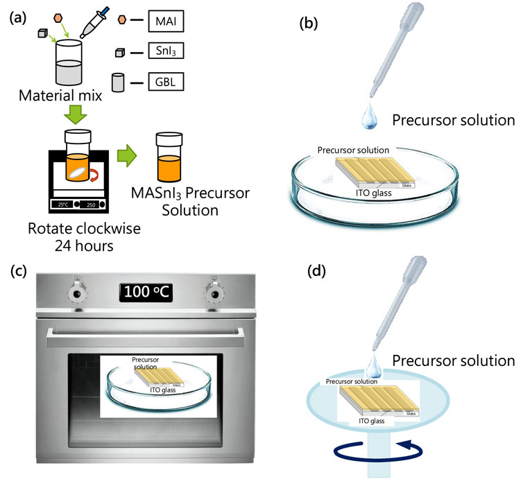
Figure 1. Process of lead-free MASnI3 perovskite metal-semiconductor-metal type photodetector: (a) precursor preparation, (b) precursor coating and (c) baking, and (d) precursor spin coating.
The crystallinities of MASnI3 perovskite on glass substrates with ITO electrodes were examined by an X-ray diffractometer (Almelo, Netherlands) with a Cu-target (λ = 1.5418 Å) source. The photoluminescence (PL) spectra and electronic properties of the photodetectors were obtained using a current source meter and spectrophotometer. The photocurrents of devices are obtained by an F-7000 fluorescence spectrophotometer with a 150-W xenon lamp.
3 Results and discussion
Figures 2a,b show the cross-sectional SEM image of MASnI3 perovskite films prepared by the ITC and spin-coating methods to check their thicknesses, respectively. The thicknesses of MASnI3 perovskite films prepared by the ITC and spin-coating methods are 20 μm and 2 μm, respectively. Figures 3a,b show the picture and top-view SEM images of MASnI3 perovskite metal-semiconductor-metal type photodetectors. A 20-μm-thick MASnI3 perovskite film with yellow color was formed on the glass substrate with an ITO electrode pattern by the inverse temperature crystallization (ITC) method. Under the observation of the top-view SEM image, as shown in Figure 3b, the morphology of the MASnI3 thin film at ×50,000 magnification shows a relatively flat pattern, but there are some flow lines and particles on the surface. The flow lines may have contributed to the MASnI3 perovskite precursor solution drying in the oven when the MASnI3 perovskite film was growing. The particles are the substances produced by the oxidation of MASnI3 perovskite material. In contrast, the MASnI3 perovskite film grown in a glove box shows a gray color, as shown in Figure 3c. It is a typical color for the MASnI3 perovskite film. The morphology of the MASnI3 perovskite film grown in a glove box is quite smooth with several small hills on the surface, as shown in Figure 3d. There are two types of growth models: the former is solvent volatilization, and the latter is a reaction between precursors. The solvent volatilization naturally results in precursor oversaturation and nucleation deposition. The surface with a small hill prepared by the spin-coating method is Stransky–Krastanov (SK) growth caused by the deposition of MASnI3 perovskite thin film, owing to the solvent volatilizing quickly.
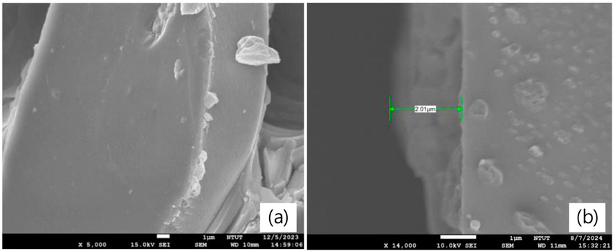
Figure 2. Cross-sectional SEM image of MASnI3 perovskite films prepared by (a) ITC and (b) spin coating, respectively.
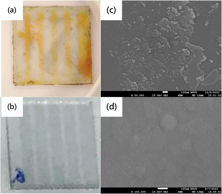
Figure 3. (a,b) Photo and (c,d) top-view SEM image of MASnI3 perovskite metal-semiconductor-metal-type photodetectors prepared in air and in a glove box, respectively.
Figure 4 shows the absorption spectra of MASnI3 perovskite on glass substrate prepared by the ITC method in air and spin coating in a glove box, respectively. Their optical absorption edges are 490 nm and 770 nm, respectively. Figure 5a shows the photoluminescence (PL) spectra of the MASnI3 perovskite on a glass substrate prepared by the ITC method in air. The peak position of the PL spectrum is approximately 470 nm, corresponding to the level transition of 2.638 eV. The band gap of MASnI3 perovskite is 1.604 eV, theoretically (Bouich et al., 2022). As shown in Figure 5b, the location of the PL peak of the MASnI3 perovskite film grown by spin coating in a glove box is 773 nm. It corresponds to the theoretical position. The broad PL spectrum of MASnI3 may contribute to the effect of the Burstein–Moss shift caused by the oxidation of MASnI3 because the material was prepared under an ambient atmosphere (Chen et al., 2006; Walukiewicz et al., 2004). Figure 5c plots the X-ray diffraction (XRD) pattern of the MASnI3 perovskite on glass substrate and shows a P-3m1 phase and a narrow full width at half maximum (FWHM) of the diffraction peak. Four main peaks appear at the diffracted peak positions 2θ = 10.2°, 19.7°, 30.0°, and 50.9°, corresponding to the crystal planes (001), (002), (003), and (005), respectively. It confirmed the formation of a single crystal of MASnI3 with trigonal P-3m1 symmetry, and the corresponding lattice parameters a = b = 9.002 Å. They are consistent with the reported values (Peng and Xie, 2020; Morimoto et al., 2022). In contrast, the structure is different from that of the sample prepared by spin coating in a glove box. It is a tetragonal crystal structure with the space group I4/mcm, as shown in Figure 5d (Walukiewicz et al., 2004). The XRD pattern shown in Figure 5d is a typical pattern of MASnI3 perovskite. However, the diffraction pattern observed in the XRD analysis does not match the reported positions of the crystal phases in the literature due to oxidation of the perovskite material (Yuan et al., 2022; Whitfield et al., 2016; Yao et al., 2017). Hence, the material prepared by the ITC method in air in this work may be an oxygen-rich MASnI3 perovskite crystal.
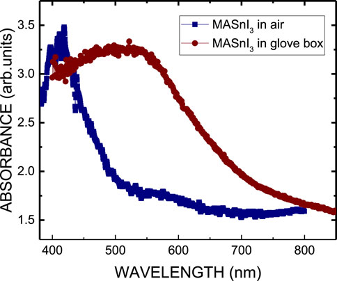
Figure 4. Absorption spectra of the MASnI3 perovskite prepared by ITC and spin coating.
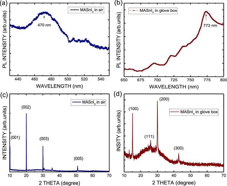
Figure 5. Photoluminescence (PL) spectra of the MASnI3 perovskite prepared by (a) ITC and (b) spin coating. XRD patterns of the MASnI3 perovskite prepared by (c) ITC and (d) spin coating, respectively.
Figure 6a plots the current–voltage (I-V) characteristics of MASnI3 perovskite metal-semiconductor-metal-type photodetectors prepared by the ITC method in air and biased from 0 V to 15 V. The MASnI3 perovskite photodetector exhibited smaller operating resistance under the light-off condition than in other situations without incident light. However, when the MASnI3 perovskite photodetector was operated in light-on conditions, the conductivity of the MASnI3 perovskite photodetector decreased. That means the defects in the MASnI3 perovskite film were filled by photo-induced electrons, such that the migration ability of electrons decreases. For the device, the largest photocurrent (4.83 × 10⁻⁶ A at 15 V) was observed when the wavelength of incident light was 700 nm. This is consistent with the band gap of the MASnI3 material. Figure 6b plots the current–voltage (I-V) characteristics of MASnI3 perovskite metal-semiconductor-metal type photodetectors prepared by the spin-coating method in a glove box and biased from 0 V to 15 V. For the device, the largest photocurrent (2.25 × 10⁻⁴ A at 15 V) was observed when the wavelength of incident light was 700 nm. The photocurrent of a device prepared in a glove box is two orders of magnitude higher than that of the device prepared by the ITC method. It may contribute to the conductivity of the MASnI3 perovskite film prepared by the spin-coating method in a glove box, which is better than that of the MASnI3 perovskite film prepared by the ITC method in a glove box due to the almost moisture-free environment and ambient oxygen.
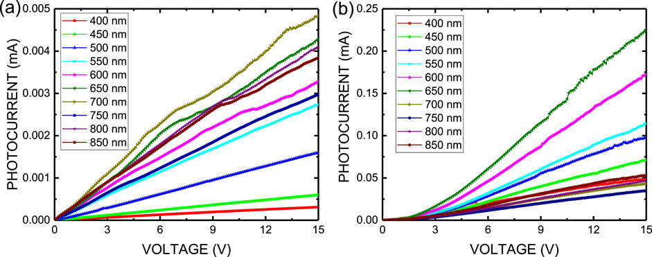
Figure 6. (a) Current–voltage (I–V) characteristics and (b) responsivity of MASnI3 perovskite metal-semiconductor-metal-type photodetectors.
Figure 7 shows the photocurrent of MASnI3 perovskite photodetectors prepared by the ITC and spin-coating methods at a bias of 15 V. Figure 8 plots the photoresponsivity of MASnI3 perovskite metal-semiconductor-metal type photodetectors prepared by the ITC and spin-coating methods, respectively, at a bias of 15 V. The photoresponsivity and detectivity of the MASnI3 perovskite photodetectors prepared by the ITC and spin-coating methods are 49.56 A/W and 1926.24 A/W under incident light of 650 nm, respectively, corresponding to 2.82 × 10¹³ and 3.28 × 10¹⁴ Jones. As shown in Figures 7, 8, the photocurrent obviously increases as the wavelength of incident light is in the range of 550–700 nm, then cuts off over 700 nm due to the absorption edge of the material. Therefore, the MASnI3 perovskite can be used to apply the photodetector with a very narrow wavelength ranging from 550 to 700 nm. Table 1 lists the optoelectronic properties of ITC and spin-coated MASnI3 photodetectors in this work. Although the ITC-prepared film exhibits better crystallinity, it results in lower device performance than the spin-coated film. It may contribute to the defect states or charge transport limitations in perovskite oxide with high resistance, according to the I-V characteristics, as shown in Figure 6. In addition, Table 2 summarizes the comparison of the detectivity of the photodetector as reported in the literature with our work. This work demonstrates the best performance.
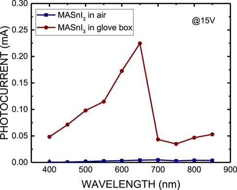
Figure 7. Photocurrent of MASnI3 perovskite metal-semiconductor-metal-type photodetectors prepared by ITC and spin coating, respectively, at a bias of 15 V.
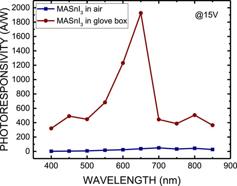
Figure 8. Photoresponsivity of MASnI3 perovskite metal-semiconductor-metal-type photodetectors prepared by ITC and spin coating, respectively, at a bias of 15 V.

Table 1. Optoelectronic properties of ITC and spin-coated MASnI3 photodetectors in this work.

Table 2. Comparison of the detectivity of the photodetectors as reported in the literature with our work.
4 Conclusion
In summary, the characteristics of two kinds of MASnI3 perovskite metal-semiconductor-metal-type photodetectors prepared by the ITC and spin-coating methods, respectively, have been demonstrated. The peaks of the photoluminescence (PL) spectrum of MASnI3 perovskite films obtained by the inversion crystallization and the spin-coating methods are 470 nm, corresponding to 2.638 eV, and 750 nm, corresponding to 1.647 eV, respectively. A Burstein–Moss shift is observed due to the introduction of oxygen. In addition, the photocurrent of a device prepared in a glove box is two orders of magnitude higher than that of the device prepared by the ITC method. The MASnI3 perovskite photodetector prepared by the ITC method in air exhibited higher operating resistance under the condition of illumination than that of the MASnI3 perovskite photodetector prepared by the spin-coating method in a glove box. That means the MASnI3 perovskite film has more defects induced by oxygen, such that the migration ability of the electrons decreases. The largest photocurrents of the MASnI3 perovskite photodetector prepared by the ITC and spin-coating methods are 4.83 × 10⁻⁶ A and 2.25 × 10⁻⁴ A at 15 V, respectively. The photocurrent increases as the wavelength of incident light is in the range of 550–700 nm, then cuts off over 700 nm due to the absorption edge of the material. Therefore, the MASnI3 perovskite can be used in the application of a photodetector with a very narrow wavelength, ranging from 600 to 700 nm. Finally, in this work, we found that the crystallinity of the sample prepared by the ITC method is better than that of the sample prepared by the spin-coating method. However, the performance of the sample prepared by the ITC method is inferior to that of the sample prepared by the spin-coating method. In addition, we found that the sample is very easy to oxidize, but it will recover after being put back into the glove box. Hence, it can be used in an oxygen-free environment.
Data availability statement
The original contributions presented in the study are included in the article/supplementary material; further inquiries can be directed to the corresponding author.
Author contributions
W-SW: conceptualization, formal analysis, investigation, resources, and writing – review and editing. Y-CC: data curation, investigation, methodology, and writing – review and editing. T-YL: conceptualization, investigation, methodology, and writing – review and editing. L-CC: conceptualization, funding acquisition, project administration, writing – original draft, and writing – review and editing.
Funding
The author(s) declare that financial support was received for the research and/or publication of this article. This research was funded by the National Science and Technology Council of Taiwan, grant number 111-2221-E-027-040-MY3.
Conflict of interest
The authors declare that the research was conducted in the absence of any commercial or financial relationships that could be construed as a potential conflict of interest.
Generative AI statement
The authors declare that no Generative AI was used in the creation of this manuscript.
Publisher’s note
All claims expressed in this article are solely those of the authors and do not necessarily represent those of their affiliated organizations, or those of the publisher, the editors and the reviewers. Any product that may be evaluated in this article, or claim that may be made by its manufacturer, is not guaranteed or endorsed by the publisher.
References
Aldamasy, M., Iqbal, Z., Li, G., Pascual, J., Alharthi, F., Abate, A., et al. (2021). Challenges in tin perovskite solar cells. Phys. Chem. Chem. Phys. 23, 23413–23427. doi:10.1039/d1cp02596a
Bouich, A., Marí-Guaita, J., Soucase, B. M., and Palacios, P. (2022). Manufacture of high-Efficiency and stable lead-free solar cells through Antisolvent Quenching Engineering. Nanomaterials 12 (17), 2901. doi:10.3390/nano12172901
Chen, L. C., Lan, W. H., Lin, R. M., Shen, H. T., and Chen, H. C. (2006). Optical properties of In2O3 oxidized from InN deposited by reactive magnetron sputtering. Appl. Sur. Sci. 252, 8438–8441. doi:10.1016/j.apsusc.2005.11.051
Chen, L. C., Tseng, Z. L., and Huang, S. K. (2016). A study of inverted-type perovskite solar cells with various composition ratios of (FAPbI3)1−x(MAPbBr3)x. Nanomaterials 6, 183. doi:10.3390/nano6100183
Hao, F., Stoumpos, C. C., Cao, D. H., Chang, R. P. H., and Kanatzidis, M. G. (2014). Lead-free solid-state organic–inorganic halide perovskite solar cells. Nat. Phot. 8, 489–494. doi:10.1038/nphoton.2014.82
Hao, F., Stoumpos, C. C., Guo, P., Zhou, N., Marks, T. J., Chang, R. P. H., et al. (2015). Solvent-mediated crystallization of CH3NH3SnI3 films for Heterojunction Depleted perovskite solar cells. J. Am. Chem. Soc. 137, 11445–11452. doi:10.1021/jacs.5b06658
Kassa, E. E., Kurniawan, A., Wu, Y. F., and Biring, S. (2025). Achieving high response of perovskite-based (MAPbI3) NH3 gas sensors using binary mixed solvent approaches. Sens. Actuators, A 383, 116116. doi:10.1016/j.sna.2024.116116
Lan, C., Dong, R., Zhou, Z., Shu, L., Li, D., Yip, S., et al. (2017). Large-scale synthesis of freestanding layer-structured PbI2 and MAPbI3 nanosheets for high-performance photodetection. Adv. Mater. 29, 1702759. doi:10.1002/adma.201702759
Lee, C. C., Kurniawan, A., Iskandar, J., Chu, C. S., and Liu, C. Y. (2025). Achieving high response of perovskite-based (MAPbI3) ammonia gas sensors at room temperature via light enhancement. J. Mater. Chem. C 13, 5140–5147. doi:10.1039/d4tc04522j
Li, Z., Jiang, L., Rong, X., Dong, Q., Dong, H., Wang, L., et al. (2022). MAPbI3 photodetectors with 4.7 MHz bandwidth and their application in organic optocouplers. J. Phys. Chem. Lett. 13, 815–821. doi:10.1021/acs.jpclett.1c04137
Mitzi, D. B., and Liang, K. (1997). Synthesis, resistivity, and thermal properties of the cubic perovskite NH2CH=NH2SnI3 and related systems. J. Solid State Chem. 134, 376–381. doi:10.1006/jssc.1997.7593
Morimoto, M., Kawano, S., Miyamoto, S., Miyazaki, K., Hayase, S., and Iikubo, S. (2022). Electronic structure and thermal conductance of the MASnI3/Bi2Te3 interface: a first-principles study. Sci. Rep. 12, 217. doi:10.1038/s41598-021-04234-3
Noel, N. K., Stranks, S. D., Abate, A., Wehrenfennig, C., Guarnera, S., Haghighirad, A. A., et al. (2014). Lead-free organic–inorganic tin halide perovskites for photovoltaic applications. Energy Environ. Sci. 7, 3061–3068. doi:10.1039/c4ee01076k
Peng, L., and Xie, W. (2020). Theoretical and experimental investigations on the bulk photovoltaic effect in lead-free perovskites MASnI3 and FASnI3. RSC Adv. 10, 14679–14688. doi:10.1039/d0ra02584d
Sabba, D., Mulmudi, H. K., Prabhakar, R. R., Krishnamoorthy, T., Baikie, T., Boix, P. P., et al. (2015). Impact of anionic Br– substitution on open circuit voltage in lead free perovskite (CsSnI3-xBrx) solar cells. J. Phys. Chem. C 119, 1763–1767. doi:10.1021/jp5126624
Saha, P., Singh, S., and Bhattacharya, S. (2024). Performance optimization of MASnI3 perovskite solar cells: insights into device architecture. Micro Nanostructures 191, 207827. doi:10.1016/j.micrna.2024.207827
Stoumpos, C. C., Malliakas, S. D., and Kanatzidis, M. G. (2013). Semiconducting tin and lead iodide perovskites with organic cations: phase transitions, high mobilities, and near-infrared photoluminescent properties. Inorg. Chem. 52, 9019–9038. doi:10.1021/ic401215x
Walukiewicz, W., Li, S. X., Wu, J., Yu, K. M., Ager III, J. W., Haller, E. E., et al. (2004). Optical properties and electronic structure of InN and In-rich group III-nitride alloys. J. Cryst. Growth 269, 119–127. doi:10.1016/j.jcrysgro.2004.05.041
Wan, J., Yu, X., Zou, J., Li, K., Chen, L., Peng, Y., et al. (2021). Lead contamination analysis of perovskite modules under simulated working conditions. Sol. Energy 226, 85–91. doi:10.1016/j.solener.2021.08.031
Whitfield, P. S., Herron, N., Guise, W. E., Page, K., Cheng, Y. Q., Milas, I., et al. (2016). Structures, phase transitions and tricritical behavior of the hybrid perovskite methyl ammonium lead iodide. Sci. Rep. 6, 35685. doi:10.1038/srep35685
Yao, Z., Xiong, Y., Kang, H., Xu, X., Guo, J., Li, W., et al. (2024). Tunable periodic nanopillar array for MAPbI3 perovskite photodetectors with improved light absorption. ACS Omega 9, 2606–2614. doi:10.1021/acsomega.3c07390
Yao, Z., Yang, Z., Liu, Y., Zhao, W., Zhang, X., Liu, B., et al. (2017). Local temperature reduction induced crystallization of MASnI3 and achieving a direct wafer production. RSC Adv. 7, 38155–38159. doi:10.1039/c7ra07101a
Yuan, Z., Zhou, J., Zhang, Y., Ma, X., Wang, J., Dong, J., et al. (2022). Growing MASnI3 perovskite single-crystal films by inverse temperature crystallization. J. Phys. Cond. Matter 34, 144009. doi:10.1088/1361-648x/ac4c64
Zhai, Y., Duan, G., Hu, J., Ly, Z., Ding, G., Zhou, Y., et al. (2024). Device-level in-sensor olfactory perception system based on array of PCBM-MAPbI3 heterostructure transistors. Adv. Funct. Mater. 34, 2406239. doi:10.1002/adfm.202406239
Keywords: perovskite, MASnI3, photodetectors, Burstein–Moss shift, oxidation
Citation: Weng W-S, Chien Y-C, Lee T-Y and Chen L-C (2025) Study of MASnI3 perovskite photodetectors prepared by the inverse temperature crystallization method in ambient atmosphere and the spin coating method in a glovebox. Front. Mater. 12:1559686. doi: 10.3389/fmats.2025.1559686
Received: 13 January 2025; Accepted: 25 April 2025;
Published: 20 May 2025.
Edited by:
Wei-Chih Lai, National Cheng Kung University, TaiwanReviewed by:
Chih Wei Chu, Academia Sinica, TaiwanBoping Yang, Hubei University of Automotive Technology, China
Copyright © 2025 Weng, Chien, Lee and Chen. This is an open-access article distributed under the terms of the Creative Commons Attribution License (CC BY). The use, distribution or reproduction in other forums is permitted, provided the original author(s) and the copyright owner(s) are credited and that the original publication in this journal is cited, in accordance with accepted academic practice. No use, distribution or reproduction is permitted which does not comply with these terms.
*Correspondence: Lung-Chien Chen, b2NlYW5AbnR1dC5lZHUudHc=