 Pratap K. Sahoo
 Nitul Rajput
 Anil Pal
 Rajesh Kumar
- 1School of Physical Sciences, National Institute of Science Education and Research (NISER) Bhubaneswar, An OCC of Homi Bhabha National Institute, Jatni, India
- 2Advanced Materials Research Center, Technology Innovation Institute, Abu Dhabi, United Arab Emirates
- 3SRM Institute of Science and Technology (Deemed to be University) Department of Physics and Nanotechnology, Kattankulathur, India
- 4Department of Physics, Materials and Device Laboratory, Indian Institute of Technology Indore, Simrol, India
Editorial on the Research Topic
Wide-bandgap oxide semiconductors: unveiling excitonic potential
Excitons, bound states of electrons and holes via Coulomb attraction, are usually short-lived and weakly bound in semiconductors like silicon, primarily because of the strong dielectric screening effects. On the other hand, in the case of wide band semiconductors, exciton binding energies are significantly enhanced, ranging from approximately 60 meV in ZnO to more than 100 meV in β-Ga2O3, which often exceeds the thermal energy at room temperature (kT ∼ 25 meV) (Das et al., 2022; Sikdar et al., 2020). This makes excitonic transitions stable and spectroscopically resolvable even at ambient conditions. Consequently, sharp excitonic absorption and emission features can be observed in photoluminescence (PL), reflectance, or ellipsometric spectra, often dominating the optical response near the band edge. The presence of the excitonic properties provides a platform for various optoelectronic applications of such materials. The various applications of excitons observed in a wide band gap oxide semiconductor is shown in the schematic of Figure 1.
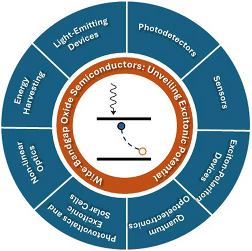
Figure 1. A schematic showing various applications of excitons present in a wide band gap oxide semiconductor.
ZnO, one of the most extensively studied wide band gap oxide semiconductors, shows three clear excitonic peaks. It has perhaps served as a model system for room-temperature excitonic lasing, and the development of polariton condensates in ZnO microcavities has propelled research into solid-state Bose–Einstein condensation. In contrast, β-Ga2O3, a fourth-generation semiconductor with a relatively broad bandgap of about 4.8 eV, has much larger exciton binding energies and anisotropic excitonic behaviour, much due to its low-symmetric monoclinic crystal structure. These characteristics, along with its high breakdown field, render Ga2O3 a highly promising material for numerous possible applications, including deep-ultraviolet photonics and high-power electronics devices (Shi and Qiao, 2022).
Despite their potential characteristics, retaining their excitonic properties can be challenging. This is due to the material issues, such as the presence of grain boundaries, native vacancies, and structural flaws. These material defects can act as nonradiative recombination sites that suppress excitonic emission. Excitons are typically more localised (Frenkel-type) and have a low radiative recombination efficiency in materials such as TiO2. This affects their utility in light-emitting applications but plays a crucial role in photocatalytic activity and charge separation processes (Olvera-Neria et al., 2024). Nevertheless, controlling crystallinity, surface states, and doping levels is essential for harnessing excitonic effects in a device.
Characterising excitonic properties in wide band gap materials has also been important for effectively understanding and designing functioning optoelectronic (excitonic) devices. Exciton lifetimes and recombination pathways can be directly measured using time-resolved photoluminescence (TRPL). High-resolution techniques such as cathodoluminescence (CL) spectroscopy and hyperspectral imaging can, on the other hand, image the exciton distribution, particularly in the vicinity of defects or interfaces.
Theoretical modelling has also been key in understanding the physics of the exciton, its origin, decay, and its engineering. State-of-the-art many-body perturbation theory, combined with the Bethe–Salpeter equation (BSE), has enabled quantitative predictions of exciton binding energies, wavefunctions, and optical spectra in excitonic wide band gap materials (Onida et al., 2002; Sun et al., 2020). These models are critical for the absolute understanding of excitonic behaviour and for guiding the design of heterostructures and quantum-confined systems.
Currently, the focus is mostly on excitonic engineering, which manipulates exciton formation, transport, and recombination through nano-structuring, strain modulation, and a dielectric environment. Quantum confinement of excitons, as provided by nanowires, quantum wells, and 2D oxides, can further improve excitonic binding and charge recombination dynamics. Integrated systems of 2D materials and oxide semiconductors can offer new opportunities for ultrafast charge separation and energy transfers. These systems are key to the fields of photovoltaics and excitonic transistors.
In summary, wide-bandgap oxide semiconductors' excitonic characteristics are essential to a variety of cutting-edge technologies and are no longer only an academic curiosity. The future of light-matter interaction will be shaped by the accurate control of excitonic dynamics as growth techniques advance and theoretical-experimental integration becomes more profound.
Author contributions
PS: Conceptualization, Resources, Supervision, Writing – original draft, Writing – review and editing. NR: Resources, Writing – original draft, Writing – review and editing. AP: Writing – review and editing. RK: Writing – review and editing.
Funding
The author(s) declare that no financial support was received for the research and/or publication of this article.
Conflict of interest
The authors declare that the research was conducted in the absence of any commercial or financial relationships that could be construed as a potential conflict of interest.
Generative AI statement
The author(s) declare that no Generative AI was used in the creation of this manuscript.
Publisher’s note
All claims expressed in this article are solely those of the authors and do not necessarily represent those of their affiliated organizations, or those of the publisher, the editors and the reviewers. Any product that may be evaluated in this article, or claim that may be made by its manufacturer, is not guaranteed or endorsed by the publisher.
References
Das, D., Escobar, F. S., Nalam, P. G., Bhattacharya, P., and Ramana, C. (2022). Excitation dependent and time resolved photoluminescence of β-Ga2O3, β-(Ga0.955Al0.045)2O3 and β-(Ga0.91In0.09)2O3 epitaxial layers grown by pulsed laser deposition. J. Luminescence 248, 118960. doi:10.1016/j.jlumin.2022.118960
Olvera-Neria, O., García-Cruz, R., Gonzalez-Torres, J., García-Cruz, L. M., Castillo-Sánchez, L. J., and Poulain, E. (2024). Strongly bound frenkel excitons on TiO2 nanoparticles: an evolutionary and DFT approach. Int. J. Photoenergy 2024 (1), 4014216. doi:10.1155/2024/4014216
Onida, G., Reining, L., and Rubio, A. (2002). Electronic excitations: density-functional versus many-body Green’s-function approaches. Rev. Mod. Phys. 74 (2), 601–659. doi:10.1103/revmodphys.74.601
Shi, F., and Qiao, H. (2022). Preparations, properties and applications of gallium oxide nanomaterials – a review. Nano Sel. 3 (2), 348–373. doi:10.1002/nano.202100149
Sikdar, M. K., Rajput, N. S., Maity, A., and Sahoo, P. K. (2020). Correlation between nonlinear optical properties and electronic band modification in cobalt-doped ZnO nanorods. Phys. Rev. Appl. 14 (1), 014050. doi:10.1103/PhysRevApplied.14.014050
Keywords: wide bandgap, oxide semiconductors, exciton, optoelectronic devices, quantum confinement
Citation: Sahoo PK, Rajput N, Pal A and Kumar R (2025) Editorial: Wide-bandgap oxide semiconductors: unveiling excitonic potential. Front. Mater. 12:1640463. doi: 10.3389/fmats.2025.1640463
Received: 03 June 2025; Accepted: 09 June 2025;
Published: 20 June 2025.
Edited and reviewed by:
Peide Ye, Purdue University, United StatesCopyright © 2025 Sahoo, Rajput, Pal and Kumar. This is an open-access article distributed under the terms of the Creative Commons Attribution License (CC BY). The use, distribution or reproduction in other forums is permitted, provided the original author(s) and the copyright owner(s) are credited and that the original publication in this journal is cited, in accordance with accepted academic practice. No use, distribution or reproduction is permitted which does not comply with these terms.
*Correspondence: Pratap K. Sahoo, cHJhdGFwLnNhaG9vQG5pc2VyLmFjLmlu