 Shiya Wen
 Shiyu Deng
 Kun Chen
 Huanjun Chen
- State Key Laboratory of Optoelectronic Materials and Technologies, Guangdong Province Key Laboratory of Display Material and Technology, School of Electronics and Information Technology, Guangzhou, China
Resonance coupling between plasmonic resonances in metallic nanostructures and excitons in two-dimensional (2D) semiconductors has attracted much recent attention. The 2D semiconductor excitons are sensitive to external stimulus, enabling active tuning on the resonance couplings by physical, such as applying electrostatic gating, thermal scanning, etc., or chemical approaches. Among the others, chemical tuning approach has the advantage of facile implementation, high efficiency, and being capable of large-area tuning. Here, we report on chemical tuning of resonance coupling in heterostructures consisted of individual gold nanorods integrated with monolayer WS2. We showed that by incubating the heterostructures into a bis (trifluoro-methane) sulfonimide (TFSI) solution, the exciton transition strength of the WS2 will be enhanced significantly. As a result, the resonance coupling in the heterostructures evolved from a weak coupling regime to a strong coupling one, with the mode splitting energy increases from 94.96 to 105.32 meV. These findings highlight the potential of chemical treatment as an efficient technique for tailoring the interactions between plasmonic nanostructures and 2D semiconductors.
Introduction
Resonance coupling refers to interactions between quantum emitters and optical cavity with spectrally overlapped resonances, which has great potentials in a variety of applications such as low-threshold lasers, ultrafast optical switches, as well as quantum information processings (Chen et al., 2013; Sanvitto and Kéna-Cohen, 2016; Baranov et al., 2018; Zheng et al., 2020; Huang et al., 2021). Basically, the resonance coupling is usually characterized by the coupling strength g (Liu et al., 2017).
where Veff is the effective mode volume of the cavity,
Currently, the control over resonance coupling between LSPRs and TMDCs excitons focuses on two aspects. The first one is by adjusting the LSPRs characteristics through tuning the composition, size, morphology, and the surrounding dielectric environment of the metal nanostructures (Liu et al., 2016; Lee et al., 2017; Kleemann et al., 2017; Wen et al., 2017; Zheng et al., 2017; Han et al., 2018; Stührenberg et al., 2018; Wen et al., 2018; Wang et al., 2019a; Chen et al., 2019; Geisler et al., 2019; Hou et al., 2019; Jiang et al., 2020; Yankovich et al., 2019; Qin et al., 2020) (see the summary on resonance coupling in different LSPR nano-/microcavity−TMDCs hybrid systems, Supplementary Table S1). The other one is by applying external stimulus to modulate the exciton behaviors of the TMDCs (Supplementary Table S1). In both ways the spectral overlap between the LSPRs and exciton transitions will be modified, and consequently the resonance coupling strengths can be tailored. In comparison with the first one, modulating resonance coupling by tuning the 2D excitons are more favorable, because the exciton transitions can be dynamically controlled in response to the external fields. For example, previous studies were able to demonstrate control of the resonance coupling strength by electrical gating and thermal scanning (Liu et al., 2016; Wen et al., 2017; Lee et al., 2017; Abid et al., 2017; Cuadra et al., 2018) (Supplementary Table S1). Chemical tuning by incubating the 2D crystals into specific acid solution has been shown to greatly improved the material’s optical properties due to reduction of the surface impurities, defects, and release of stress between the substrate and 2D crystals (Amani et al., 2016a; Han et al., 2016; Hu et al., 2018; Zhu et al., 2019). In particular, it was demonstrated that exciton emission of 2D MoS2 and WS2 can be significantly enhanced by the chemical treatment of organic super acid bis (trifluoromethane) sulfonimide (TFSI) (Amani et al., 2015; Amani et al., 2016a; Amani et al., 2016b). In comparison with other tuning methods, chemical tuning approach has the advantage of facile implementation, high efficiency, and being capable of large-area tuning. However, to the best of our knowledge, tuning the resonance coupling between LSPRs and excitons in TMDCs through a chemical approach is yet to be explored.
Here, we report the chemical tuning of resonance coupling in heterostructures composed of individual gold nanorods integrated with monolayer WS2. LSPRs of gold nanorods enable sub-diffraction confinement of electromagnetic fields at the surface of WS2, making them coherently coupling with the 2D excitons in the monolayer. Resonance coupling evidenced by clear anti-crossing behaviors can be observed from the pristine individual heterostructures. The extracted mode splitting energy is 94.96 meV, indicating a weak coupling regime. Upon incubating the heterostructures into the TFSI solution, the transition dipole moment of the WS2 exciton can be strongly enhanced. This will strengthen the resonance coupling and give rise to a mode splitting energy of 105.32 meV. Such a value suggests that the resonance coupling has approached the strong coupling regime. The observed increments in mode splitting and associated enhancement of exciton transition dipole moment are in good agreement with calculated results using coupled oscillator model (COM).
Experimental
Chemicals and Materials
HAuCl4.3H2O (Au > 99.9%) was purchased from Aladdin (Shanghai, China). TFSI (95%) was purchased from Macklin (Shanghai, China). Cetyltrimethylammonium bromide (CTAB: >99%), silver nitrate (AgNO3: >99%), sodium oleate (NaOL: >97%), and l-ascorbic acid (AA: >99%) were purchased from Sigma-Aldrich. Sodium borohydride (NaBH4: >96%) was purchased from Acros Organics (Shanghai, China). The HCl (37 wt% in water) is of analytical grade, which was purchased from Aladdin (Shanghai, China). Monolayer WS2 was grown directly onto a silicon substrate capped with a 300-nm thick oxide layer (Nanjing MKNANO Tech. Co., Ltd.). All chemicals were used without further purification. Deionized water (18.2 MΩ cm) was used during the preparations of the gold nanorods and heterostructures.
Sample Preparations
Gold nanorods were grown using a seed-mediated method with binary surfactant mixture (Ye et al., 2013; Zhuang et al., 2018; Xu et al., 2020). The seed solution was prepared by mixing 2.5 ml HAuCl4 (0.5 mM) and 2.5 ml CTAB (0.2 M) solution in a 30-ml glass vial. Then 0.3 ml NaBH4 solution (0.01 M) was added to the mixture under vigorous stirring for 2 min until the color of the solution changed from yellow to brownish yellow. The seed solution was aged at room temperature for 30 min before use. To prepare the growth solution, 0.9 g of CTAB and 0.1234 g of NaOL was dissolved in DI water (∼50°C) in a 25 ml glass conical flask, kept undisturbed for 15 min at 27°C after adding AgNO3 solution (2.4 ml, 4 mM). Subsequently, HAuCl4 (25 ml, 1 mM) was added to the solution and stirred for 90 min. A certain amount of HCl solution was added to the growth solution and stirred for 15 min to adjust the PH. Afterwards the AA solution (0.125 ml, 0.064 mM) was added with vigorous stirring for 30 s. A certain amount of the prepared seed solution was injected into the growth solution under vigorous stirring for 30 s. The mixture was then left undisturbed for 12 h for the growth of the gold nanorods. The aspect ratio of the nanorods can be continuously adjusted by varying the amounts of the seed solution as well as pH of the growth solution (Jiang et al., 2020).
To fabricate the heterostructures, the monolayer WS2 was first transferred onto another SiO2 substrate for releasing the stress (Gurarslan et al., 2014; Xu et al., 2015; McCreary et al., 2016). Specifically, a layer of polystyrene (PS) was spin-coated (3,300 rpm, 1 min) onto the as-grown WS2, followed by a baking process at 120°C for 1 h. After scribing the PS film with a scalpel, the sample was placed into DI water to lift off the PS film adhered with the WS2 monolayer from the SiO2/Si substrate. The PS film was then placed onto the target SiO2 substrate. Afterwards, the PS film was removed with toluene solution after baking the sample at 120°C for 1 h. The heterostructures were formed by drop-casting gold nanorod aqueous solutions with different nanorod aspect ratios onto the transferred monolayer WS2 flake.
Chemical Treatment
Certain amounts of TFSI were dissolved into 20 ml acetone to make TFSI solutions with different concentrations. The SiO2 substrates with the gold nanorods and heterostructures were incubated into the TFSI solutions for different 30 s. Afterwards, the substrate was taken out from the TFSI solution and annealed on a hot plate at 50°C for 1 min.
Characterizations
Raman and photoluminescence (PL) spectra were measured using a micro-Raman spectrometer (inVia Reflex, Renishaw). The samples were excited by a laser of 532 nm. Extinction spectra of the aqueous gold nanorod samples with different aspect ratios were measured on a UV/visible/near-infrared spectrophotometer (U-4100, HITACHI). Atomic force microscope (AFM, NTEGRA Spectra, NT-MDT) was employed to characterized the morphologies and thicknesses of the samples. The scattering spectra of the various individual gold nanorods and heterostructures were recorded on a home-built dark-field microscope. The microscope consists of an optical microscope (Olympus BX51) integrated with a broadband white light source, a monochromator (Acton SpectraPro 2,360), and a charge-coupled device camera (Princeton Instruments Pixis 400BR_eXcelon). During the measurements, the CCD was maintained at −50°C. A dark-field objective (×100, numerical aperture 0.80) was employed for both illuminating the heterostructures and collecting the scattered light.
Numerical simulations
Scattering spectra of the individual gold nanorods and heterostructures were simulated using the finite-difference time-domain (FDTD) method. A single gold nanorod was modeled as a cylinder capped with a hemisphere at each end. The monolayer WS2 was modeled as dielectric layer with a thickness of 1 nm. An individual heterostructure is constructed by placing a gold nanorod onto the WS2 layer, with a gap of 1 nm in between (Wen et al., 2017; Jiang et al., 2020). The bulk dielectric function of the gold was used (Johnson and Christy, 1972). The dielectric function of the pristine and TFSI treated monolayer WS2 was modeled using the Lorentzian model (Yilei et al., 2014), with parameters determined from their PL spectra (see the discussion below). A dielectric constant of 2.25 was used for the SiO2 substrate. The diameters of the gold nanorods were set from 34.48 to 61.93 nm, and the lengths were varied from 77.26 to 125.60 nm. These parameters correspond to nanorod aspect ratios ranging from 1.47 to 2.66. All of the nanorods and heterostructures were excited by a linearly polarized plane wave, with the polarization along the longitudinal axes of the nanorods. Mesh size of 0.5 nm was set around the nanorods.
Results and Discussion
The as-prepared gold nanorods have uniform size and shape distributions (Figure 1A; Supplementary Figure S1), where two types of LSPR modes can be observed from their extinction spectra (Figure 1B; Supplementary Figure S1M). They are the transverse (TPM) and longitudinal (LPM) LSPR modes, which are associated with electron oscillations along the transverse and longitudinal directions of the nanorods, respectively. In our study, the LPM is considered because its resonance wavelengths (frequencies) can be synthetically tuned by tailoring the aspect ratio of the gold nanorods (Figure 1B; Supplementary Figure S1M), which is defined as the nanorod length divided by the diameter (Chen et al., 2013). The commercial monolayer WS2 flake was grown by chemical vapor deposition (CVD) method, where an intrinsic tensile strain exists between the flake and SiO2 substrate (McCreary et al., 2016). Such a strain can significantly suppress the exciton transition of the WS2. Therefore, the monolayer WS2 was first transferred to another SiO2 substrate to release the tensile strain (Figure 1I) (Gurarslan et al., 2014; Xu et al., 2015). The thickness of the transferred WS2 flake can be determined by AFM topography, which is 1.0 nm as shown in Figures 1C,D. The monolayer WS2 exhibits two evident Raman peaks at 352 cm−1 and 419 cm−1 (Figure 1E), which correspond to the E2g and A1g modes of WS2, respectively (Cong et al., 2014). In addition, 2D Raman intensity mapping (monitored at 352 cm−1) across the entire flake is uniform, indicating a good crystallinity of the monolayer WS2 (Figure 1F). The exciton luminescence of the monolayer WS2 was characterized by PL spectroscopy. As shown in Figure 1G, the pristine monolayer WS2 exhibits a PL peak at 2.016 eV (615 nm), with a linewidth (ℏγex) of 95.1 meV. The PL intensity mapping across the entire flake reveals excellent uniformity of the exciton transition (Figure 1H).
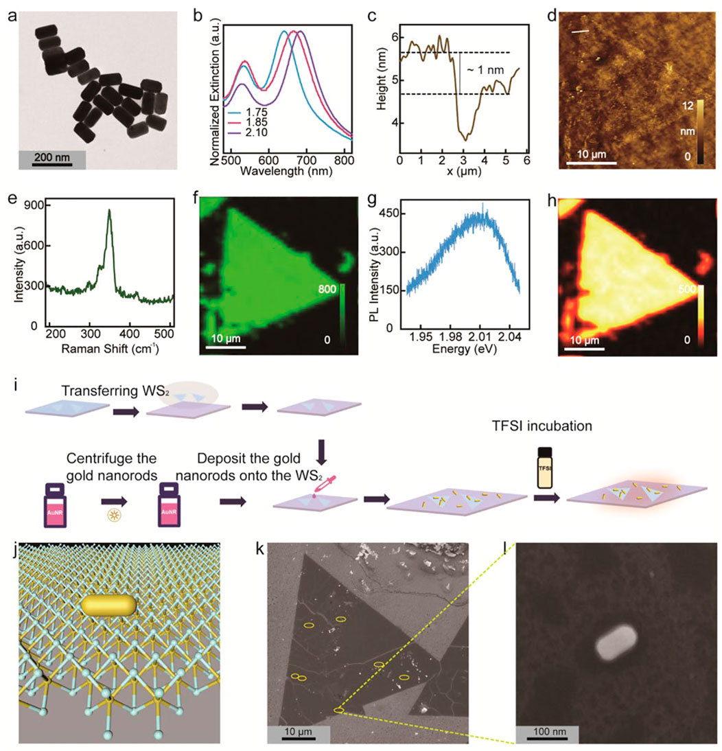
FIGURE 1. Characterizations of gold nanorods and monolayer WS2. (A) Transmission electron microscopy (TEM) image of gold nanorods. (B) Normalized extinction spectra of three typical gold nanorod samples with different nanorod aspect ratios. Numbers next to the colored lines indicate the aspect ratios. (C, D) AFM topography (C) and image (D) of the monolayer WS2. The topography shown in (C) is collected along the white solid line shown in (D). (E) Raman spectrum of the monolayer WS2 flake. (F) 2D Raman intensity mapping of the sample corresponding to (D). The mapping is monitored at 352 cm−1. (G) PL spectrum of the monolayer WS2 flake. (H) 2D PL intensity mapping of the WS2 flake corresponding to (D). The mapping is monitored at emission peak of 2.016 eV. (I) Schematic showing processes of fabricating the heterostructures and TFSI treatment. (J) Schematic showing the individual gold nanorod−monolayer WS2 heterostructure. (K) Scanning electron microscope (SEM) image of nanorods distributing sparsely onto the WS2 flake. Yellow circles indicate the individual heterostructures. (L) SEM image of an individual gold nanorod−monolayer WS2 heterostructure.
To construct the heterostructures (Figure 1J), gold nanorods were centrifuged twice to remove the capping agents CTAB and redispersed into deionized water. Afterwards, gold nanorods with different aspect ratios were mixed and drop-casted respectively onto a clean SiO2 substrate and the monolayer WS2 flake that was transferred onto another SiO2 substrate (Figure 1I). The concentration of the nanorod solution was controlled to ensure sparse nanorod distribution onto the SiO2 substrate and WS2 flake (Figure 1K), enabling subsequent characterizations of an individual heterostructure (Figure 1L). Due to the organic residues surrounding the nanorod, the spacing between the nanorod and WS2 surface (or the clean SiO2 substrate surface) is ∼1 nm.
Chemical treatment was realized by incubating the heterostructures into TFSI solutions (Figure 1I). To ascertain the optimum TFSI concentration (CTFST) for the incubation, a typical monolayer WS2 flake was subjected to chemical incubation with different CTFST, whereby its PL spectra was measured and compared. The incubation time is set as 30 s. In comparison with the pristine WS2 monolayer, those experiencing TFSI incubations exhibit evidently enhanced PL intensity (Supplementary Figure S2A−S2F). In addition, the chemical treatment also affects the PL spectral shape of the WS2 (Supplementary Figure S2G). The modifications of the PL intensity and spectra are dependent on the CTFST. Specifically, the peak intensity of the PL increases steadily and reaches a maximum at a CTFST of 3 mg/ml (Supplementary Figure S2H). Afterwards, the PL intensity reduces as the CTFST is further increased. To quantify the exciton emission of the monolayer WS2 upon TFSI incubation, the PL spectra were fitted using a lineshape of,
where F and ℏγ are respectively scale factor and the PL spectrum linewidth. In particular, F is proportional to exciton transition dipole moment, while ℏγ is proportional to the damping rate of the exciton. ℏωex is the exciton transition energy. As shown in Supplementary Figure S2I, the PL spectra of the pristine WS2 and WS2 flake incubated in TFSI solution of 0.1 mg/ml can be well described using Eq. 2. By applying Eq. 2 to fit the spectra shown in Supplementary Figure S2G, it can be clearly seen that the extracted ℏωex (ℏγ) first increases (decreases) and then saturates for CTFST ≥ 0.1 mg/cm (Supplementary Figure S2J and S2K). In contrast, the parameter F first increases against the CTFST, and then decreases when the concentration is larger than 3 mg/ml (Supplementary Figure S2L). On the other hand, the LSPRs of the individual gold nanorods are almost invariant when they are incubated in TFSI solution of 0.1 mg/ml, as manifested from their dark-field (DF) scattering spectra (Supplementary Figure S3A). However, when the CTFST is increased, redshift of the LSPR peak and broadening of the DF scattering spectra can be observed (Supplementary Figure S3B and S3C). These results clearly suggest that a TFST solution of CTFST = 0.1 mg/ml should be employed for the incubation, whereby the exciton emission can be chemically modified without changing the LSPR characteristics of the nanorods.
To ensure that the TFSI incubation will not deteriorate the structure and morphology of the monolayer WS2, AFM and Raman spectroscopy characterizations were conducted on the WS2 flake after incubated in 0.1 mg/ml TFSI solution. As shown in Figure 2A–C, both of the thickness and topography of the sample after TFSI treatment are similar to those of the pristine one. In addition, the treated WS2 flake exhibit similar and enhanced Raman spectrum compared to that of the pristine one (Figure 2D). The enhanced Raman intensity recorded at 352 cm−1 (E2g mode) distributes uniformly over the whole flake (Figures 2E,F). These results indicate that the TFSI incubation can help remove the surface defects and impurities of the monolayer WS2 flake (Amani et al., 2016a). This can suppress the annihilation centers for excitons and give rise to uniformly enhanced exciton emission across the whole flake (Figure 2G–I). The PL intensity of the incubated sample is about 5.57 times larger than that of the pristine one (Figure 2G). In addition, the PL linewidth is also reduced by ∼51% in the incubated sample, which is only 46 meV (Figure 2G; Supplementary Figure S2I).
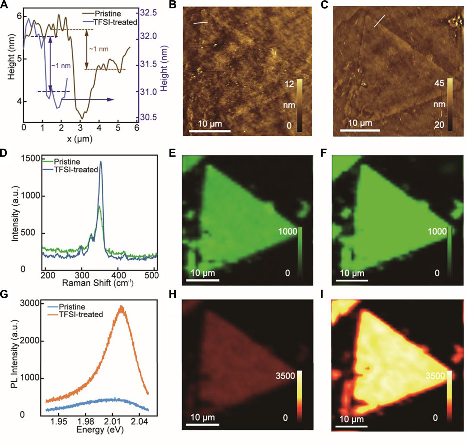
FIGURE 2. Characterizations of the monolayer WS2 flake after incubation in TFSI solution of 0.1 mg/ml. (A) Topographies of the pristine (brown line) and incubated (blue line) WS2 flake. (B, C) AFM images of the pristine (B) and incubated (C) WS2 flake. The topographies are drawn along the white lines shown in (B) and (C). (D) Raman spectra of the monolayer WS2 before (green line) and after (blue line) TFSI incubation. (E, F) 2D Raman intensity mappings of the WS2 flake before (E) and after (F) the TFSI incubation. The Raman mappings are monitored at 352 cm−1. (G) PL spectra of the monolayer WS2 before (blue) and after (orange) the TFSI incubation. (H, I) 2D PL intensity mappings of the WS2 flake before (H) and after (I) the TFSI incubation. The PL mappings are recorded at 615 nm.
The resonance coupling in the various individual plasmonic nanostructures was characterized using single-particle DF scattering spectroscopy, which can rule out the average effect from the ensemble measurements (Zengin et al., 2015; Santhosh et al., 2016; Cuadra et al., 2018; Stührenberg et al., 2018). Figure 3A (upper panel) shows DF scattering spectrum from a typical gold nanorod with an aspect ratio of 1.75, where a well-defined peak centering at 2.03 eV can be observed. The scattering maximum corresponds to LPM of the nanorod, which is in resonance with the exciton emission of the WS2 (2.016 eV) (Figure 3A, green curve in middle panel). Upon formation of the heterostructure, the DF scattering spectrum was modified significantly due to the resonance coupling between the LPM and exciton transition. Two scattering maxima separated by a spectral dip corresponding to the exciton transition energy of WS2 can be observed (Figure 3A, blue curve in the lower panel). Moreover, the two scattering peaks are strongly dependent on the detuning energy defined as
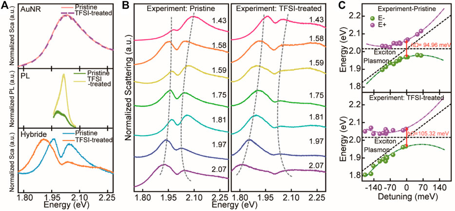
FIGURE 3. Resonance coupling in individual gold nanorod−WS2 heterostructures. (A) Scattering spectra of an individual gold nanorod (upper), PL spectra of the monolayer WS2 (middle), and scattering spectra of an individual heterostructure (lower). (B) DF scattering spectra from different individual heterostructures. Left panel: pristine heterostructures. Right panel: heterostructures upon 0.1 mg/ml-TFSI incubation. Numbers next to the curves indicate the aspect ratios of the gold nanorods in the heterostructures. (C) Scattering peaks as a function of the detuning energy between the LPM and exciton transition energy. Upper panel: pristine heterostructures. Lower panel: heterostructures upon 0.1 mg/ml-TFSI incubation. The horizontal and diagonal black dashed lines indicate the exciton transition energy and LPM energy, respectively. The colored symbols are extracted from the scattering spectra shown in (B). The colored dashed lines are polynomial fittings.
Numerical FDTD simulations were then employed to verify the experimental findings. To that end, simulation architectures were set according to the SEM images of the individual gold nanorods and various heterostructures. A pivotal parameter employed in the simulations is the dielectric function of the monolayer WS2. In our study, the Lorentzian model was used to describe the dielectric functions of the pristine and TFSI treated monolayer WS2. Specifically, the dielectric function can be expressed as (Yilei et al., 2014),
where ε∞ = 18.1 is the high-frequency permittivity (Yilei et al., 2014). For the pristine and TFSI treated WS2 flakes, ℏωex and ℏγex are respectively adopted from the fittings of the corresponding PL spectra using Eq. 2 (Supplementary Figure S4 and Supplementary Table S2). Parameter f is the oscillator strength that is related to the exciton transition dipole moment. For the pristine WS2, f is set as 0.523 (Yilei et al., 2014), while for the TFSI treated WS2, it is calculated according to f = 0.523 F’/F0, with F0 and F′ the scale factors of the WS2 before and after incubation in 0.1 mg/ml TFSI solution (Supplementary Table S2). The dielectric functions of the pristine and TFSI-treated WS2 calculated by Eq. 3 are shown in Supplementary Figure S4, which exhibit similar lineshapes. However, due to the strengthened exciton transition dipole moment by the chemical treatment, the f is enlarged by 1.53 times, giving rise to enhancement of the magnitudes for both of the real and imaginary parts (Supplementary Table S2).
With the knowledge of ε, the scattering spectra of the various structures are readily calculated. As shown in Figure 4A (upper and middle panels), the simulated scattering spectra of an individual gold nanorod (with an aspect ratio of 2.04) and the associated heterostructure can well-reproduce the experimental spectra (Figure 3A, upper and lower panels). Additionally, the simulated spectral evolutions against the ∆ for the various heterostructures agree well with the experimental ones (Figure 4B, left panel). Anti-crossing behavior can also be identified from the simulated scattering spectra. It should be noted that there is a discrepancy on the scattering dip position between the experimental measurements and simulations. This can be understood because the dielectric function of the WS2 used in the simulations was measured on samples obtained by mechanical exfoliation, while the monolayer WS2 employed in the measurements was grown by the CVD method. It is known that the ℏωex can vary between the CVD-grown and exfoliated samples (Amani et al., 2014; Krustok et al., 2017), giving rise to differences in the corresponding dielectric functions.
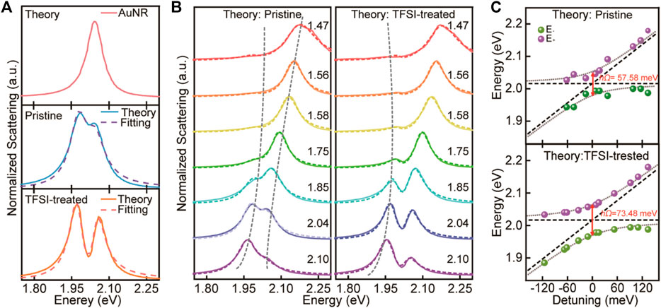
FIGURE 4. Numerical simulations and COM analyses of the resonance coupling. (A) FDTD simulated scattering spectra of an individual gold nanorod (upper panel), an individual pristine heterostructure (middle panel), and individual TFSI-treated heterostructure (lower panel). Dashed lines are fitting curves using COM model. (B) Simulated scattering spectra from different individual heterostructures. Left: pristine heterostructures. Right: heterostructures upon chemical treatment. Numbers next to the curves indicate the aspect ratios of the gold nanorods in the heterostructures. Dashed lines are COM fitting curves. (C) Scattering peaks extracted from the COM model as a function of the detuning energy between the LPM and exciton transition energy. Upper: pristine heterostructures. Lower: heterostructures upon chemical treatment. The horizontal and diagonal black dashed lines indicate the exciton transition energy and LPM energy, respectively. The colored symbols are extracted from the COM fitting spectra shown in (B). The dotted curves are guide for the eyes.
The dependence of the two scattering peaks on the ∆ was further investigated. As shown in Figure 3C (upper panel), the two peaks always exist when the ∆ is tuned from negative to positive values. In addition, the two peaks show a distinct anti-crossing behavior against ∆ (Figure 3C, upper panel), featuring the occurrence of the resonance coupling. The energy difference (ℏΩ) between the two scattering maxima at zero detuning characterizes the coupling strength (see the following discussion) (Baranov et al., 2018; Törmä and Barnes, 2015). With the knowledge of ℏΩ, the regime of the resonance coupling (i.e., weak coupling, moderate coupling, or strong coupling) can be ascertained. As shown in Figure 3C (upper panel), the Ω can determined as 94.96 meV. Such a value is smaller than (ℏγpl+ℏγex)/2 (123.78 meV) (Supplementary Table S3), suggesting that the resonance coupling between the LPM and WS2 exciton transition is a Fano interference process, i.e., a weak coupling regime (Wu et al., 2010; Leng et al., 2018).
The TFSI treatment can enhance the exciton transition dipole moment as well as reduce the damping of the exciton (middle panel of Figure 3A and Supplementary Figure S4A). These can in turn affect the dielectric function and thereafter the resonance coupling between the LPM and WS2 exciton. As shown in Figure 3A (lower panel), the intensity ratio between the two scattering maxima in the incubated sample (orange) is distinctly different from that of the pristine sample (blue). The chemical tuning on the resonance coupling can be manifested more evidently from the evolution of the scattering spectrum against the nanorod aspect ratio. As shown in Figure 3B (right panel), for the incubated heterostructures, the energy differences between the two scattering peaks become larger for the incubated sample as compared to those of the pristine counterparts (Figure 3B, left panel). In addition, the spectral dip corresponding to the exciton transition also becomes deeper. The experimental spectral shapes and evolvements of the incubated heterostructures agree well with the simulated results (Figure 4A, lower panel and Figure 4B, right panel). Most importantly, the ℏΩ deduced from the anti-crossing curves increases to 105.32 meV after the chemical treatment. Such a value is a bit larger than (ℏγpl+ℏγex)/2 (104.6 meV) (Supplementary Supplementary Table S3), indicating that the resonance coupling has approached the strong coupling regime (Liu et al., 2015; Törmä and Barnes, 2015). The two scattering peaks can thereafter be ascribed to occurrence of mode splitting.
To further discuss the underlying physics governing the chemical tuning of the resonance coupling, mode analyses on the simulated scattering spectra were performed using a coupled oscillator model (COM). The COM is widely employed for analyzing resonance coupling between quantum emitters and plasmonic nanostructures (Wu et al., 2010; Leng et al., 2018; Wang et al., 2019b). Specifically, the scattering spectrum of an individual gold nanorod−monolayer WS2 heterostructure can be written as (Wu et al., 2010; Wang et al., 2019b),
where g is the coupling strength between LPM and WS2 exciton. For zero detuning, i.e., ℏωex = ℏωpl, the heterostructure exhibits two eigenstates with energies (frequencies) as,
The two eigenstates are manifested as the two scattering peaks in the DF scattering spectra. Therefore, the energy difference between the two scattering peaks at ∆ = 0 can be expressed as,
Eq. 6 provides the direct relationship between the energy difference Ω and coupling strength g. When 2g < (ℏγpl+ℏγex)/2, Fano interferences between the exciton transition and LPM takes place, while for 2 g > (ℏγpl+ℏγex)/2, mode splitting occurs (Wu et al., 2010; Itoh et al., 2014; Dufferwiel et al., 2015; Wang et al., 2019b). As shown in Figures 4A,B (dashed lines), Eq. 4 can well-describe the FDTD simulated scattering spectra. Moreover, for both the pristine and chemically-treated heterostructures, the scattering peaks extracted from the fitting spectra using Eq. 4 follow clear anti-crossing behaviors (Figure 4C). The obtained ℏΩ at zero detuning are respectively 57.58 and 73.48 meV (Supplementary Table S4). Although these values are both smaller than the corresponding experimental ones, the enhancement of ℏΩ by chemical treatment agrees well with the experimental measurements. Most importantly, the COM results indicate that for the pristine heterostructure the two scattering peaks are due to the Fano interference because the 2 g (57.58 meV) is smaller than (ℏγpl+ℏγex)/2 (86.93 meV). In contrast, for the chemically-treated heterostructure, the 2 g = 73.48 meV > (ℏγpl+ℏγex)/2 = 65.84 meV can be observed. Therefore, the chemical treatment can tune the heterostructure from a weak coupling regime into a strong coupling one, which is corroborated with the experimental findings.
With the COM fitting results, the mechanisms on the chemical tuning of resonance coupling can be understood. Specifically, TFSI solution can effectively passivate/repair the defects and impurities on the monolayer WS2. This can enhance the exciton transition dipole moment and reduce the damping rate. A larger transition dipole moment can generate a stronger oscillator strength, and a smaller damping rate can lead to a longer exciton lifetime. These two outcomes will both enhance the resonance coupling between the LPM and exciton transition, making the system transfer from a weak coupling regime into a strong coupling regime.
We need to point out that the chemical tuning approach reported in our current study is very slow, which is a main drawback in our proposal. The tuning speed is about 30 s, because the monolayer WS2 has to be incubated into the TFSI solution for such a long time to remove and repair the surface defects. Currently, it is a challenge to accelerate the chemical tuning on the resonance coupling, which is limited by the intrinsic materials properties in the monolayer WS2. We anticipate that the tuning speed can be improved by increasing the incubation temperature, which can help accelerate the chemical reactions responsible for defects repair. Another issue is the stability of the chemical tuning approach. Generally, the defects removed by surface passivation will be recovered after exposure to water and commonly used organic solvents. Therefore, to improve the stability of the chemical tuning, preservation and encapsulation of the heterostructure should be considered. Previous studies have demonstrated that some polymer with environmental stability and high optical transparency, such as CYTOP and amorphous perfluorinated polymer, have been applied to encapsulate the TMDCs (Kim et al., 2017). They can therefore be employed to encapsulate the incubated heterostructures to extend the tuning effect on the resonance coupling.
Conclusion
In summary, we successfully demonstrate chemical tuning on the resonance coupling between LSPR in individual gold nanorod and 2D excitons in monolayer WS2 flake. By incubating the heterostructures into TFSI solution, defects and impurities in WS2 will be reduced, which can enhance the exciton transition dipole moment and reduce the damping rate. These will lead to stronger coupling strengths between the LSPR and 2D excitons. Consequently, the splitting energies between the two DF scattering peaks become larger for the incubated individual heterostructures. The mode splitting energy increases from 94.96 to 105.32 meV, indicating that the resonance coupling evolves from a weak coupling regime to a strong coupling one. These results can be verified with those obtained from FDTD simulations and COM analyses. We believe that the findings in our study can on one hand provide an efficient approach for tailoring the interactions between plasmonic nanostructures and 2D semiconductors, and on the other hand help to improve our understanding on light−matter interactions at nanoscale.
Data Availability Statement
The original contributions presented in the study are included in the article/supplementary material, further inquiries can be directed to the corresponding author.
Author Contributions
HC and SD conceived the study and supervised the project.SW prepared the heterostructures, characterized the resonance coupling, conducted the FDTD simulations, and performed the COM analyses. SD helped prepare the samples and characterizations. SW, SD, KC, HC, and SD. analyzed the data and discussed the results. The article was written through contributions of all authors. All authors have given approval to the final version of the manuscript.
Funding
We acknowledge support from the National Key Basic Research Program of China (grant no. 2019YFA0210203), the National Natural Science Foundation of China (grant nos. 91963205 and 11904420), Guangdong Basic and Applied Basic Research Foundation (grant no. 2020A1515011329). H.C. acknowledges the support from Changjiang Young Scholar Program.
Conflict of Interest
The authors declare that the research was conducted in the absence of any commercial or financial relationships that could be construed as a potential conflict of interest.
Publisher’s Note
All claims expressed in this article are solely those of the authors and do not necessarily represent those of their affiliated organizations, or those of the publisher, the editors and the reviewers. Any product that may be evaluated in this article, or claim that may be made by its manufacturer, is not guaranteed or endorsed by the publisher.
Supplementary Material
The Supplementary Material for this article can be found online at: https://www.frontiersin.org/articles/10.3389/fmats.2021.744275/full#supplementary-material
References
Abid, I., Chen, W., Yuan, J., Bohloul, A., Najmaei, S., Avendano, C., et al. (2017). Temperature-Dependent Plasmon-Exciton Interactions in Hybrid Au/MoSe2 Nanostructures. ACS Photon. 4 (7), 1653–1660. doi:10.1021/acsphotonics.6b00957
Amani, M., Burke, R. A., Ji, X., Zhao, P., Lien, D.-H., Taheri, P., et al. (2016). High Luminescence Efficiency in MoS2 Grown by Chemical Vapor Deposition. Acs Nano 10 (7), 6535–6541. doi:10.1021/acsnano.6b03443
Amani, M., Chin, M. L., Mazzoni, A. L., Burke, R. A., Najmaei, S., Ajayan, P. M., et al. (2014). Growth-substrate Induced Performance Degradation in Chemically Synthesized Monolayer MoS2 Field Effect Transistors. Appl. Phys. Lett. 104 (20), 203506. doi:10.1063/1.4873680
Amani, M., Lien, D.-H., Kiriya, D., Xiao, J., Azcatl, A., Noh, J., et al. (2015). Near-unity Photoluminescence Quantum Yield in MoS2. Science 350 (6264), 1065–1068. doi:10.1126/science.aad2114
Amani, M., Taheri, P., Addou, R., Ahn, G. H., Kiriya, D., Lien, D.-H., et al. (2016). Recombination Kinetics and Effects of Superacid Treatment in Sulfur- and Selenium-Based Transition Metal Dichalcogenides. Nano Lett. 16 (4), 2786–2791. doi:10.1021/acs.nanolett.6b00536
Baranov, D. G., Wersäll, M., Cuadra, J., Antosiewicz, T. J., and Shegai, T. (2018). Novel Nanostructures and Materials for strong Light-Matter Interactions. Acs Photon. 5 (1), 24–42. doi:10.1021/acsphotonics.7b00674
Chen, H., Shao, L., Li, Q., and Wang, J. (2013). Gold Nanorods and Their Plasmonic Properties. Chem. Soc. Rev. 42 (7), 2679–2724. doi:10.1039/c2cs35367a
Chen, X., Wang, H., Xu, N.-S., Chen, H., and Deng, S. (2019). Resonance Coupling in Hybrid Gold Nanohole-Monolayer WS2 Nanostructures. Appl. Mater. Today 15, 145–152. doi:10.1016/j.apmt.2019.01.004
Chernikov, A., Berkelbach, T. C., Hill, H. M., Rigosi, A., Li, Y., Aslan, O. B., et al. (2014). Exciton Binding Energy and Nonhydrogenic Rydberg Series in Monolayer WS2. Phys. Rev. Lett. 113 (7), 076802. doi:10.1103/PhysRevLett.113.076802
Cong, C., Shang, J., Wu, X., Cao, B., Peimyoo, N., Qiu, C., et al. (2014). Synthesis and Optical Properties of Large-Area Single-Crystalline 2D Semiconductor WS2 Monolayer from Chemical Vapor Deposition. Adv. Opt. Mater. 2 (2), 131–136. doi:10.1002/adom.201300428
Cuadra, J., Baranov, D. G., Wersäll, M., Verre, R., Antosiewicz, T. J., and Shegai, T. (2018). Observation of Tunable Charged Exciton Polaritons in Hybrid Monolayer WS2−Plasmonic Nanoantenna System. Nano Lett. 18 (3), 1777–1785. doi:10.1021/acs.nanolett.7b04965
Dufferwiel, S., Schwarz, S., Withers, F., Trichet, A. A. P., Li, F., Sich, M., et al. (2015). Exciton-polaritons in van der Waals heterostructures embedded in tunable microcavities. Nat. Commun. 6 (1), 8579. doi:10.1038/ncomms9579
Geisler, M., Cui, X., Wang, J., Rindzevicius, T., Gammelgaard, L., Jessen, B. S., et al. (2019). Single-Crystalline Gold Nanodisks on WS2 Mono- and Multilayers for Strong Coupling at Room Temperature. ACS Photon. 6 (4), 994–1001. doi:10.1021/acsphotonics.8b01766
Gurarslan, A., Yu, Y., Su, L., Yu, Y., Suarez, F., Yao, S., et al. (2014). Surface-Energy-Assisted Perfect Transfer of Centimeter-Scale Monolayer and Few-Layer MoS2 Films onto Arbitrary Substrates. ACS Nano 8 (11), 11522–11528. doi:10.1021/nn5057673
Han, H.-V., Lu, A.-Y., Lu, L.-S., Huang, J.-K., Li, H., Hsu, C.-L., et al. (2016). Photoluminescence Enhancement and Structure Repairing of Monolayer MoSe2 by Hydrohalic Acid Treatment. ACS Nano 10 (1), 1454–1461. doi:10.1021/acsnano.5b06960
Han, X., Wang, K., Xing, X., Wang, M., and Lu, P. (2018). Rabi Splitting in a Plasmonic Nanocavity Coupled to a WS2 Monolayer at Room Temperature. ACS Photon. 5 (10), 3970–3976. doi:10.1021/acsphotonics.8b00931
Han, Y., Liu, Y., Su, C., Chen, X., Li, B., Jiang, W., et al. (2021). Hierarchical WS2-WO3 Nanohybrids with P-N Heterojunctions for NO2 Detection. ACS Appl. Nano Mater. 4 (2), 1626–1634. doi:10.1021/acsanm.0c03094
Han, Y., Liu, Y., Su, C., Wang, S., Li, H., Zeng, M., et al. (2019). Interface Engineered WS2/ZnS Heterostructures for Sensitive and Reversible NO2 Room Temperature Sensing. Sensors Actuators B: Chem. 296, 126666. doi:10.1016/j.snb.2019.126666
Hou, S., Tobing, L. Y. M., Wang, X., Xie, Z., Yu, J., Zhou, J., et al. (2019). Manipulating Coherent Light-Matter Interaction: Continuous Transition between Strong Coupling and Weak Coupling in MoS2 Monolayer Coupled with Plasmonic Nanocavities. Adv. Opt. Mater. 7 (22), 1900857. doi:10.1002/adom.201900857
Hu, Z., Wu, Z., Han, C., He, J., Ni, Z., and Chen, W. (2018). Two-dimensional Transition Metal Dichalcogenides: Interface and Defect Engineering. Chem. Soc. Rev. 47, 3100–3128. doi:10.1039/c8cs00024g
Huang, W., Sun, F., Zheng, Z., Folland, T. G., Chen, X., Liao, H., et al. (2021). Van der Waals Phonon Polariton Microstructures for Configurable Infrared Electromagnetic Field Localizations. Adv. Sci. 8 (13), 2004872. doi:10.1002/advs.202004872
Itoh, T., Yamamoto, Y. S., Tamaru, H., Biju, V., Wakida, S.-i., and Ozaki, Y. (2014). Single-molecular Surface-Enhanced Resonance Raman Scattering as a Quantitative Probe of Local Electromagnetic Field: The Case of strong Coupling between Plasmonic and Excitonic Resonance. Phys. Rev. B 89 (19), 195436. doi:10.1103/physrevb.89.195436
Jiang, Y., Wang, H., Wen, S., Chen, H., and Deng, S. (2020). Resonance Coupling in an Individual Gold Nanorod-Monolayer WS2 Heterostructure: Photoluminescence Enhancement with Spectral Broadening. ACS Nano 14 (10), 13841–13851. doi:10.1021/acsnano.0c06220
Johnson, P. B., and Christy, R. W. (1972). Optical Constants of the Noble Metals. Phys. Rev. B 6 (12), 4370–4379. doi:10.1103/physrevb.6.4370
Kim, H., Lien, D.-H., Amani, M., Ager, J. W., and Javey, A. (2017). Highly Stable Near-Unity Photoluminescence Yield in Monolayer MoS2 by Fluoropolymer Encapsulation and Superacid Treatment. ACS Nano 11 (5), 5179–5185. doi:10.1021/acsnano.7b02521
Kleemann, M.-E., Chikkaraddy, R., Alexeev, E. M., Kos, D., Carnegie, C., Deacon, W., et al. (2017). Strong-coupling of WSe2 in Ultra-compact Plasmonic Nanocavities at Room Temperature. Nat. Commun. 8 (1), 1296. doi:10.1038/s41467-017-01398-3
Krustok, J., Kaupmees, R., Jaaniso, R., Kiisk, V., Sildos, I., Li, B., et al. (2017). Local Strain-Induced Band gap Fluctuations and Exciton Localization in Aged WS2 Monolayers. AIP Adv. 7 (6), 065005. doi:10.1063/1.4985299
Lee, B., Liu, W., Naylor, C. H., Park, J., Malek, S. C., Berger, J. S., et al. (2017). Electrical Tuning of Exciton-Plasmon Polariton Coupling in Monolayer MoS2 Integrated with Plasmonic Nanoantenna Lattice. Nano Lett. 17 (7), 4541–4547. doi:10.1021/acs.nanolett.7b02245
Leng, H., Szychowski, B., Daniel, M.-C., and Pelton, M. (2018). Strong Coupling and Induced Transparency at Room Temperature with Single Quantum Dots and gap Plasmons. Nat. Commun. 9, 4012. doi:10.1038/s41467-018-06450-4
Liu, R., Zhou, Z.-K., Yu, Y.-C., Zhang, T., Wang, H., Liu, G., et al. (2017). Strong Light-Matter Interactions in Single Open Plasmonic Nanocavities at the Quantum Optics Limit. Phys. Rev. Lett. 118 (23), 237401. doi:10.1103/physrevlett.118.237401
Liu, W., Lee, B., Naylor, C. H., Ee, H.-S., Park, J., Johnson, A. T. C., et al. (2016). Strong Exciton-Plasmon Coupling in MoS2 Coupled with Plasmonic Lattice. Nano Lett. 16 (2), 1262–1269. doi:10.1021/acs.nanolett.5b04588
Liu, X., Galfsky, T., Sun, Z., Xia, F., Lin, E.-c., Lee, Y.-H., et al. (2015). Strong Light-Matter Coupling in Two-Dimensional Atomic Crystals. Nat. Photon 9 (1), 30–34. doi:10.1038/nphoton.2014.304
Luo, H., Shi, J., Liu, C., Chen, X., Lv, W., Zhou, Y., et al. (2021). Design of P-P Heterojunctions Based on CuO Decorated WS2 Nanosheets for Sensitive NH3 Gas Sensing at Room Temperature. Nanotechnology 32 (44), 445502. doi:10.1088/1361-6528/ac1800
McCreary, K. M., Hanbicki, A. T., Singh, S., Kawakami, R. K., Jernigan, G. G., Ishigami, M., et al. (2016). The Effect of Preparation Conditions on Raman and Photoluminescence of Monolayer WS2. Sci. Rep. 6 (1), 35154. doi:10.1038/srep35154
Qin, J., Chen, Y. H., Zhang, Z., Zhang, Y., Blaikie, R. J., Ding, B., et al. (2020). Revealing Strong Plasmon-Exciton Coupling between Nanogap Resonators and Two-Dimensional Semiconductors at Ambient Conditions. Phys. Rev. Lett. 124 (6), 063902. doi:10.1103/PhysRevLett.124.063902
Ramasubramaniam, A. (2012). Large Excitonic Effects in Monolayers of Molybdenum and Tungsten Dichalcogenides. Phys. Rev. B, Condensed matter 86 (11), 2757–2764. doi:10.1103/physrevb.86.115409
Santhosh, K., Bitton, O., Chuntonov, L., and Haran, G. (2016). Vacuum Rabi Splitting in a Plasmonic Cavity at the Single Quantum Emitter Limit. Nat. Commun. 7, ncomms11823. doi:10.1038/ncomms11823
Sanvitto, D., and Kéna-Cohen, S. (2016). The Road towards Polaritonic Devices. Nat. Mater 15 (10), 1061–1073. doi:10.1038/nmat4668
Schneider, C., Glazov, M. M., Korn, T., Höfling, S., and Urbaszek, B. (2018). Two-dimensional Semiconductors in the Regime of strong Light-Matter Coupling. Nat. Commun. 9 (1), 2695. doi:10.1038/s41467-018-04866-6
Stührenberg, M., Munkhbat, B., Baranov, D. G., Cuadra, J., Yankovich, A. B., Antosiewicz, T. J., et al. (2018). Strong Light-Matter Coupling between Plasmons in Individual Gold Bi-pyramids and Excitons in Mono- and Multilayer WSe2. Nano Lett. 18 (9), 5938–5945. doi:10.1021/acs.nanolett.8b02652
Sun, J., Li, Y., Hu, H., Chen, W., Zheng, D., Zhang, S., et al. (2021). Strong Plasmon-Exciton Coupling in Transition Metal Dichalcogenides and Plasmonic Nanostructures. Nanoscale 13 (8), 4408–4419. doi:10.1039/d0nr08592h
Törmä, P., and Barnes, W. L. (2015). Strong Coupling between Surface Plasmon Polaritons and Emitters: a Review. Rep. Prog. Phys. 78 (1), 013901. doi:10.1088/0034-4885/78/1/013901
Wang, H., Wen, J., Wang, W., Xu, N., Liu, P., Yan, J., et al. (2019). Resonance Coupling in Heterostructures Composed of Silicon Nanosphere and Monolayer WS2: A Magnetic-Dipole-Mediated Energy Transfer Process. ACS Nano 13 (2), 1739–1750. doi:10.1021/acsnano.8b07826
Wang, S., Le-Van, Q., Vaianella, F., Maes, B., Eizagirre Barker, S., Godiksen, R. H., et al. (2019). Limits to Strong Coupling of Excitons in Multilayer WS2 with Collective Plasmonic Resonances. ACS Photon. 6 (2), 286–293. doi:10.1021/acsphotonics.8b01459
Wen, J., Wang, H., Wang, W., Deng, Z., Zhuang, C., Zhang, Y., et al. (2017). Room-Temperature Strong Light-Matter Interaction with Active Control in Single Plasmonic Nanorod Coupled with Two-Dimensional Atomic Crystals. Nano Lett. 17 (8), 4689–4697. doi:10.1021/acs.nanolett.7b01344
Wen, J. X., Wang, H., Chen, H. J., Deng, S. Z., and Xu, N. S. (2018). Room-temperature strong Coupling between Dipolar Plasmon Resonance in Single Gold Nanorod and Two-Dimensional Excitons in Monolayer WSe2. Chin. Phys B 27 (9), 096101. doi:10.1088/1674-1056/27/9/096101
Wu, X., Gray, S. K., and Pelton, M. (2010). Quantum-dot-induced Transparency in a Nanoscale Plasmonic Resonator. Opt. Express 18 (23), 23633–23645. doi:10.1364/oe.18.023633
Xu, Y., Zhou, B., Zhuang, C., Zhou, J., Chen, H., and Deng, S. (2020). High‐Aspect‐Ratio Plasmonic Heterostructures for In Vivo Enhanced Optical Coherence Tomography Imaging in the Second Near‐Infrared Biological Window. Adv. Opt. Mater. 8 (15), 2000384. doi:10.1002/adom.202000384
Xu, Z.-Q., Zhang, Y., Lin, S., Zheng, C., Zhong, Y. L., Xia, X., et al. (2015). Synthesis and Transfer of Large-Area Monolayer WS2 Crystals: Moving toward the Recyclable Use of Sapphire Substrates. ACS Nano 9 (6), 6178–6187. doi:10.1021/acsnano.5b01480
Yang, Y., liu, W. G., Lin, Z. T., Pan, R. H., Gu, C. Z., and Li, J. J. (2021). Plasmonic Hybrids of Two-Dimensional Transition Metal Dichalcogenides and Nanoscale Metals: Architectures, Enhanced Optical Properties and Devices. Mater. Today Phys. 17, 100343. doi:10.1016/j.mtphys.2021.100343
Yankovich, A. B., Munkhbat, B., Baranov, D. G., Cuadra, J., Olsén, E., Lourenço-Martins, H., et al. (2019). Visualizing Spatial Variations of Plasmon-Exciton Polaritons at the Nanoscale Using Electron Microscopy. Nano Lett. 19 (11), 8171–8181. doi:10.1021/acs.nanolett.9b03534
Ye, X., Zheng, C., Chen, J., Gao, Y., and Murray, C. B. (2013). Using Binary Surfactant Mixtures to Simultaneously Improve the Dimensional Tunability and Monodispersity in the Seeded Growth of Gold Nanorods. Nano Lett. 13 (2), 765–771. doi:10.1021/nl304478h
Yilei, L., Alexey, C., Xian, Z., Albert, R., and Heather, M. H. (2014). Measurement of the Optical Dielectric Function of Monolayer Transition-Metal Dichalcogenides: MoS2, MoSe2, WS2, and WSe2. Phys. Rev. B 90 (20), 205422.
Zengin, G., Wersäll, M., Nilsson, S., Antosiewicz, T. J., Käll, M., and Shegai, T. (2015). Realizing Strong Light-Matter Interactions between Single-Nanoparticle Plasmons and Molecular Excitons at Ambient Conditions. Phys. Rev. Lett. 114 (15), 157401. doi:10.1103/physrevlett.114.157401
Zheng, D., Li, Y., Chen, W., Fu, T., Sun, J. W., Zhang, S. P., et al. (2019). The Novel Plasmonics-Transition Metal Dichalcogenides Hybrid Nanostructures. Sci. Sin-phys Mech. As 49 (12), 124205. doi:10.1360/sspma-2019-0111
Zheng, D., Zhang, S., Deng, Q., Kang, M., Nordlander, P., and Xu, H. (2017). Manipulating Coherent Plasmon-Exciton Interaction in a Single Silver Nanorod on Monolayer WSe2. Nano Lett. 17 (6), 3809–3814. doi:10.1021/acs.nanolett.7b01176
Zheng, Z., Sun, F., Huang, W., Jiang, J., Zhan, R., Ke, Y., et al. (2020). Phonon Polaritons in Twisted Double-Layers of Hyperbolic van der Waals Crystals. Nano Lett. 20 (7), 5301–5308. doi:10.1021/acs.nanolett.0c01627
Zhu, Y., Yi, H., Hao, Q., Liu, J., Ke, Y., Wang, Z., et al. (2019). Scalable Synthesis and Defect Modulation of Large Monolayer WS2 via Annealing in H2S Atmosphere/thiol Treatment to Enhance Photoluminescence. Appl. Surf. Sci. 485, 101–107. doi:10.1016/j.apsusc.2019.04.168
Keywords: WS2, resonance couplings, gold nanorods, plasmon resonances, chemical tunings
Citation: Wen S, Deng S, Chen K, Chen H and Deng S (2021) Chemical Tuning on Resonance Coupling in Gold Nanorod−Monolayer WS2 Heterostructures. Front. Mater. 8:744275. doi: 10.3389/fmats.2021.744275
Received: 20 July 2021; Accepted: 06 September 2021;
Published: 22 September 2021.
Edited by:
Qiaoliang Bao, Soochow University, ChinaReviewed by:
Zhi Yang, Shanghai Jiao Tong University, ChinaLi Li, East China Normal University, China
Copyright © 2021 Wen, Deng, Chen, Chen and Deng. This is an open-access article distributed under the terms of the Creative Commons Attribution License (CC BY). The use, distribution or reproduction in other forums is permitted, provided the original author(s) and the copyright owner(s) are credited and that the original publication in this journal is cited, in accordance with accepted academic practice. No use, distribution or reproduction is permitted which does not comply with these terms.
*Correspondence: Huanjun Chen, Y2hlbmhqOEBtYWlsLnN5c3UuZWR1LmNu