 Dong Hyun Lee1
 Taehyun Park2
 Taeho Jeong3Youngkyun Jung3
 Junghee Park3Nackyong Joo3
 Uiyeon Won3
 Hocheon Yoo1*
- 1Department of Electronic Engineering, Gachon University, Seongnam, Gyeonggi, Republic of Korea
- 2Department of Chemical and Biological Engineering, Gachon University, Seongnam, Gyeonggi, Republic of Korea
- 3Electronic Devices Research Team, Hyundai Motor Group, Uiwang, Gyeonggi, Republic of Korea
Molybdenum disulfide (MoS2) has great potential for next-generation electronic devices. On the other hand, stable doping methods are required to adjust its physical properties so MoS2 can be utilized in practical applications, such as transistors and photodetectors. On the other hand, a conventional doping method based on ion implantation is incompatible with 2D MoS2 because of the damage to the lattice structures of MoS2. This paper presents an n-type doping method for MoS2 field-effect transistors (FETs) using a poly (vinylidene fluoride-co-trifluoroethylene) (P (VDF-TrFE)) and polar polymer. The dipole moment of P (VDF-TrFE) provides n-type doping on MoS2 FETs. The polar phase formation in dopant films enhances the doping effects, and the relationship between phase transition and n-type doping states was investigated using optical and electrical characterization methods. Under the optimal doping conditions, the doped MoS2 FET achieved an improved field effect mobility of 34.4 cm2 V−1s–1, a negative shift in the threshold voltage by −25.6 V, and a high on-current of 21 μA compared to the pristine MoS2 FET.
1 Introduction
Since the first application of graphene in an electronic device, two-dimensional (2D) materials, including transition-metal dichalcogenides (TMDs), hexagonal boron nitride (h-BN), and Mxenes, have been highlighted in various research fields. Among the 2D materials family, MoS2 is a promising next-generation semiconducting material owing to its mechanical flexibility (Samy et al., 2021), appropriate energy band gap (Kim et al., 2020), high carrier mobility (Shen et al., 2020), and high transparency (Lee et al., 2013). Therefore, MoS2 may have a wide range of applications, including displays (Choi et al., 2020; Hwangbo et al., 2022), chemical sensors (Pham et al., 2019; Kumar et al., 2020), optical detectors (Gant et al., 2019; Woo et al., 2021a), and integrated circuit devices (Lin et al., 2020; Wang et al., 2022).
Despite this potential, issues, such as variation in physical properties based on the number of layers and a high contact resistance caused by the high Schottky barrier between the MoS2 and metal electrodes, are a problem in the application field of MoS2-based electronic devices (Yoo et al., 2018). In general, doping is the most common technique for controlling the properties of semiconductors. Ion implantation is the most common technique for silicon-based electronics because it allows for delicate control and good quality in the doping process of thick silicon. On the other hand, this approach is incompatible with 2D MoS2 because it causes significant damage to the lattice structure and defects in atomically thin layers.
Various attempts have been reported to overcome the limitations of the above-described conventional doping technology. For example, the surface functionalization of MoS2 can be considered an alternative approach. Depending on the donor or acceptor states, p-type or n-type doping effects are achieved on MoS2 devices (Pak et al., 2019). In doped transistors, however, a large reduction in the subthreshold swing was often observed due to the formation of trap states during the functionalization. Substoichiometric metal oxide dopant films fabricated by atomic layer deposition (ALD) can also provide efficient doping effects on MoS2 FETs (Woo et al., 2021b). Metal oxide dopant layers exhibit high stability without degradation, but the on/off current ratios or subthreshold swings of doped devices are typically reduced (McClellan et al., 2021). Furthermore, the ALD-based doping approach requires a complex and high-cost process. Doping results for small molecule dopants have a high degree of freedom regarding the charge carrier concentration and doping types (Wang et al., 2020). Nevertheless, this method has stability issues in dopant films (McClellan et al., 2021) in the viewpoints of air exposure or thermal degradation. To maintain a doping effect in practical environments, the stability of the dopant layer should be secured. In general, the fixed physical or chemical properties of dopant layers provide high chemical resistance. However, fixed charges or states of dopant films have a limitation in terms of controllable doping effect with the variation of dipole moments. A doping approach that simultaneously provides characteristics such as controllability, reliability, and stability, which are important for the practical use of TMD-based electronic devices, is still lacking.
Along this line, this paper presents a controllable, reliable, and thermally stable n-type doping approach for MoS2 FETs by forming a polar P(VDF-TrFE) polymer dopant layer. P(VDF-TrFE) is one of the most promising piezoelectric materials with good chemical stability (Choi et al., 2015) and dielectric properties (Meng et al., 2020). The dopant film was fabricated using a simple spin-coating method without any functionalization, which reduces the possibilities of trap-state formation. The top dopant layer provides n-type doping effects to the bottom MoS2 based on dipole moments, which can be controlled further by the crystalline phases via the melting and recrystallization process. As the concentration of polar phases in dopant films increased, the proposed device exhibited improved electrical performances, such as on-current, on/off ratio, and field effect mobility. Furthermore, the uniformity and reproducibility of the proposed approach were investigated with 8 different devices. The n-type doping mechanism on MoS2 was examined according to the phase transition of dopant films using comprehensive electrical characterization, Raman and photoluminescence (PL) spectroscopies.
2 Materials and methods
2.1 The fabrication process of MoS2 FET
A 300 nm of silicon dioxide film was formed using a dry oxidation process on a heavily boron-doped silicon substrate with 500–550 μm of thickness (supplied from Namkang Hi-Tech Inc., South Korea). Heavily boron-doped Si/SiO2 substrates were sonicated for 10 min with isopropyl alcohol, and ethanol, subsequently and then blown with nitrogen gas on Si/SiO2 substrates to remove residue. Semiconducting MoS2 layers were mechanically exfoliated from the MoS2 crystals (supplied from HQ Graphene, Netherlands) using adhesive 3 M Scotch tapes and transferred onto heavily boron-doped Si/SiO2 substrates. At this time, the average thickness of 7 pristine MoS2 flakes is 25.6 nm ± 12.3 nm. The source and drain electrodes were patterned on as-transferred MoS2 flakes using the conventional photolithography method (EVG 620, EV Group, Austria). To pattern the source and drain electrodes, the image-reverse photoresist AZ 5214E (supplied from Clariant Corp., United States) was spin-coated on Si/SiO2 substrates with MoS2 crystals transferred. Then, the solvent was removed from the spin-coated photoresist by annealing process on a hot plate at 110°C for 1 min. The exposure process was performed on photoresist-coated Si/SiO2 substrates using a photomask with a mesh structure. To remove the source/drain-patterned photoresist, phase transition of the photoresist was performed by annealing on a hot plate at 120°C for 150 s. Subsequently, photoresist-patterned Si/SiO2 substrates were dipped in AZ 300 MIF developer (supplied by Az Electronic Materials Co. Ltd., United States) for 19 s to remove the photoresist with the source/drain patterned. To deposit the source/drain electrodes, the photoresist-patterned Si/SiO2 substrates were mounted in a vacuum evaporation equipment (SHE-8T-500, Samhan Vacuum Development, South Korea). The 20 nm of titanium (Ti) for the adhesion layer was deposited by electron-beam evaporation method in a vacuum condition of 3 × 10⁻⁶ mTorr. Then. Subsequently, 100 nm of gold (Au) was deposited on the entire surface of photoresist-patterned Si/SiO2 substrates using the thermal evaporation method. Ti/Au-deposited Si/SiO2 substrates were immersed in 60°C of acetone and the source and drain electrodes were patterned using the lift-off method. At last, the fabricated MoS2 FET was dried using nitrogen gas. The length and width of the fabricated MoS2 FET were 10.7 and 12.9 μm, respectively. The proposed device consisted of a bottom-gate/top-contact structure.
2.2 Remote n-type doping process
The dopant solution was prepared by dissolving P(VDF-TrFE) in acetonitrile (anhydrous, 99.8%) at a concentration of 7 mg mL−1. The as-prepared solution was aged for 24 h for stabilization. The dopant solution was spin-coated on MoS2 FETs at 500 rpm and 30 s conditions. The doped MoS2 FETs were annealed at 60°C on a hotplate for 10 min after spin coating to remove the residual solvent. The effects of P(VDF-TrFE) phase transition were examined by sequential annealing of the as-doped devices at 100, 200, and 300°C. In addition, the P(VDF-TrFE)-doped MoS2 FETs with 10 min annealed had slowly cooling to 60°C.
2.3 Characterization methods
The phase transition of dopant P(VDF-TrFE) and lattice vibration of the MoS2 flakes were observed by Raman and PL spectroscopy with an in-house-built, combined spectroscopy system at room temperature. Both Raman and PL spectroscopy measurements were performed using a SYCERITY 1024 × 256-OE TE cooled CCD detector (HORIBA Scientific, Japan) for UV-VIS-NIR regimes and a HORIBA Jobin Yvon NanoLog equipped with a laser excitation wavelength of 532 nm. All spectra were collected with an optical microscope (BX43-32P01HAL, Olympus, Japan) with the ×100 objective lens (N.A. 0.9). Water contact angles of P(VDF-TrFE) films annealed at different conditions were measured with the Contact angle meter (DSA100, KRÜSS Scientific Instruments Inc., Germany) All electrical characterization of MoS2 FETs in this work was measured in air-ambient condition (RH = 21% and temperature = 23.6°C) using a Keithley 4,200 parameter analyzer (Keithley Instruments Inc., United States) installed in a probe station (MS-Tech, South Korea). In addition, the thermal stability of the P(VDF-TrFE)-doped MoS2 FET was measured using a probe station chamber connected to a Keithley 4,200 parameter. A hot chuck mounted in the probe station chamber applies a temperature of up to 100°C to the devices.
3 Result and discussion
3.1 Characterization of n-type doping effects on MoS2 FETs
First, the changes in morphological and optical properties of the MoS2 FET according to the remote n-type doping process were examined. Figure 1A illustrates the n-type doping process and molecular structure of the components. Optical microscopy photographs according to n-type doping states (Figures 1B, C) showed no observable decomposition in MoS2 flakes, proving that the proposed solution coating method is an appropriate n-type doping approach without causing significant damage to the thin MoS2 semiconductor. The optical characterization of the MoS2 region revealed the effect of the n-type doping process. The optical characterization of the MoS2 region revealed the effect of the doping process with Raman spectroscopy (Figure 1D). To clearly observe the shape and shift in A1g and E2g1 peaks, we have performed Lorentzian function fitting for each raw data point. As shown in Figure 1D, the A1g and E2g1 modes provide information on the out-of-plane strain and in-plane vibration, respectively (Zhou et al., 2014). The A1g and E2g1 peaks are both red-shifted in the n-type doped MoS2 sample compared to the pristine MoS2. The specific positions of A1g peak in the fitted line were 406.8 cm-1 and 407.7 cm-1 at n-type doped MoS2 and pristine MoS2, respectively. The E2g1 peak positions were extracted with the values of 380.9 cm-1 and 382.1 cm-1 for n-type doped and bare MoS2 films. As reported in previous studies, heavy n-type doping shifts the Fermi level near the conduction band, causing interactions between the continuum of electronic states and optical phonons (Sahoo and Kale, 2019; Schauble et al., 2020; Tanwar et al., 2022). The above electron-phonon interaction (i.e., Fano interaction) arises owing to appropriate matching between discrete phonon energy and electron continuum energy by heavy doping and photoexcited carriers. Resonance of the two energies leads to constructive or destructive interference and results in perturbed line shapes at Raman spectral parameters (Tanwar et al., 2022). In the case of A1g mode, peak shift is the main indicator of the n-type doing of MoS2 (Chakraborty et al., 2012; Miller et al., 2015; Manamel et al., 2020; Krishnan K et al., 2021). Furthermore, the increased asymmetric ratio in Raman peaks provide the quantitative information of doping induced Fano interaction (Sahoo and Kale, 2019; Schauble et al., 2020; Tanwar et al., 2022). To quantitatively compare the MoS2 E2g1 peak asymmetric ratios depending on the n-type doping procedure, we extracted the peak parameters such as full width at half maximum (FWHM, Г), Half-width in pre-maximum side (γL), and Half-width in post-maximum side (γR) by fitting the raw data points with bi-Gaussian function. As shown in Supplementary Figure S1, the asymmetric ratio (γL/γR) of pristine MoS2 was 1.01, which is almost close to 1 and reveals the peak is symmetric. In contrast, the asymmetric ratio of the n-type doped MoS2 was calculated to be 0.95, suggesting that the peak asymmetry increased through the electron-phonon interaction (i.e., Fano interaction) with the doped state. The above-mentioned asymmetry in E2g1 Raman peaks were further investigated through Fano fitting which defined by the following Eq. 1 (Schauble et al., 2020).
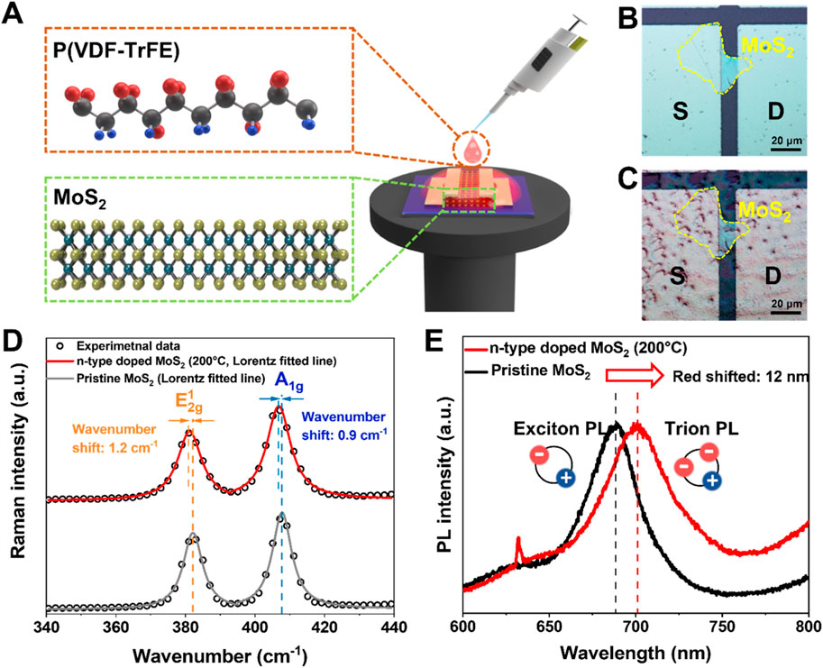
FIGURE 1. (A) Schematic diagram of dopant, MoS2, and doping process. Optical micrographs of the MoS2 FETs: (B) pristine MoS2 FET and (C) P(VDF-TrFE)-doped MoS2 FETs. (D) Raman spectroscopic analysis results of n-type doped and pristine MoS2 flakes. The Lorentzian fits are represented with solid lines. (E) PL emission spectra of MoS2 flakes according to the n-type doping states under 532 nm excitation.
Where ao is the prefactor, ω is frequency, ωp is bare phonon frequency, γ is the linewidth, and q is the symmetry parameter depends on electron-phonon coupling strength. As previously reported in literatures, a lower absolute value |q| indicates greater asymmetry and heavier doping (Nickel et al., 2000; Schauble et al., 2020). The calculated q values in the Fano profiles for pristine and n-type doped MoS2 were 29.89 and 12.25, respectively (Supplementary Figure S2). The lower q value for the n-type doped MoS2 suggests a greater asymmetry and a heavier doped state compared to the pristine MoS2.
The changes in the electronic states of the MoS2 region after n-type doping were also discovered in the PL spectrum (Figure 1E). The PL emission peak of doped MoS2 was red-shifted by 12 nm compared to the pristine MoS2. The PL emission of MoS2 was attributed to exciton (X, peak at ∼ 690 nm) and trion (X−1, peak at ∼ 702 nm) recombination (Brill et al., 2021). Because trions are more negatively charged than excitons, an increase in trion-related PL emission shows that the MoS2 region is more negatively charged (n-doped). The PL peak was red-shifted towards the trion PL emission direction when the P(VDF-TrFE) film was fabricated on the MoS2. This result confirms the n-type doping effect through dopant fabrication. The effect of n-type doping on MoS2 observed in the PL measurements was verified through the electrical characterization of the device.
As mentioned in the introduction, certain organic materials, such as self-assembled monolayers (SAMs), and polar polymers, can provide n-type doping effects to control the electrical characteristics of MoS2 FETs (Li et al., 2013; Kang et al., 2015; Maity et al., 2017). The dipole effect could change the electrical characteristics of a MoS2 FET in the case of the P(VDF-TrFE) film coated with the surface of the MoS2 semiconductor. Figures 2A, B present 3D schematic diagrams of pristine and MoS2 FETs doped with a P(VDF-TrFE) solution. An as-coated P(VDF-TrFE) thin film was formed after 10-min annealing to evaporate the solvent. Subsequently, annealing was performed at 100, 200, and 300°C using a hotplate for 10 min. The electrical characteristics of the MoS2 FETs were measured to assess the n-type doping effect of P(VDF-TrFE). Figure 2C shows the transfer curves of a pristine MoS2 FET and P(VDF-TrFE)-doped MoS2 FET. The drain voltage of 1 V and the gate voltage range of −40 V–40 V were applied to two types of MoS2 FETs to collect the transfer curve. The pristine MoS2 FET with typical n-type behavior showed an on-current of 8.7 μA, and a field effect mobility of 26.9 cm2 V−1s–1. In addition, the P(VDF-TrFE) doping effect was maximized according to the annealing temperature. The on-current and field effect mobility of the P(VDF-TrFE)-doped MoS2 FET (100°C) increased significantly to 12 μA and 30.7 cm2 V−1s–1, respectively. The P(VDF-TrFE)-doped MoS2 FET (200°C) with the most improved n-type operation has a 21 μA on-current and 34.4 cm2 V−1s–1 of mobility. The crystal structure of P(VDF-TrFE) has α, β, and γ phases and can be controlled by annealing temperature. The P(VDF-TrFE) annealed at 200°C has high alignment due to the formation of the ß phase. The ß phase of P(VDF-TrFE) induces a strong dipole moment and enhances the n-type operation of the MoS2 FET. On the other hand, the electrical characteristics of the P(VDF-TrFE)-doped MoS2 FET (300°C) are deteriorating, with an on-current of 1.6 μA and a field effect mobility of 12.4 cm2 V−1s–1, respectively. The dipole moment of P(VDF-TrFE) induced on the surface of the MoS2 semiconductor was weakened because the alignment of the P(VDF-TrFE) was lower. Figure 2D shows the output curves of pristine MoS2 FET and doped MoS2 FET (200°C). The output curves of the MoS2 FETs were measured by applying a drain voltage of 0 V–10 V and a gate voltage of −10 V–40 V. The P(VDF-TrFE) has the effect of increasing the on-current of MoS2 FETs with increased drain current in the same gate voltage range. Figure 2E presents the contact resistance and channel resistance of a pristine MoS2 FET and a P(VDF-TrFE) doped MoS2 FET extracted by the G-function method (Liu et al., 2015; Jiang et al., 2019). The channel resistance and contact resistance of the extracted MoS2 FET decrease as the annealing temperature increases. The channel resistance and contact resistances of the pristine MoS2 FET are 0.14 MΩ and 7.4 kΩ, respectively. When MoS2 FET is doped with P(VDF-TrFE) and subsequently to an annealing process at 100°C, the channel resistance (0.55 MΩ) and contact resistance (5.8 kΩ) are significantly reduced. The P(VDF-TrFE)-doped pristine MoS2 FET (200°C) exhibits the lowest channel resistance (0.51 MΩ) and contact resistance (2.9 kΩ). Low channel resistance and contact resistance increase the field effect mobility, on-current and, lower the operating voltage of MoS2 FET. On the other hand, the channel resistance (1.04 MΩ) and contact resistance (8.6 kΩ) of the P(VDF-TrFE)-doped pristine MoS2 FET (300°C) increased compared to pristine MoS2 FET. The P(VDF-TrFE) doping effect lowers the Schottky barrier in the MoS2 FET and induces a low contact resistance. Owing to the dipole effect of P(VDF-TrFE), the n-type behavior of the doped MoS2 FET was enhanced. Figure 2F shows the energy band diagram of a pristine MoS2 FET. The energy band of pristine MoS2 makes it difficult to tunnel electrons into the electrode. On the other hand, P(VDF-TrFE) brings the conduction band and Fermi level of MoS2 closer (Figure 2G). Hence, the dipole moment of P(VDF-TrFE) shifts the energy band of MoS2 downward, facilitating electron tunneling.
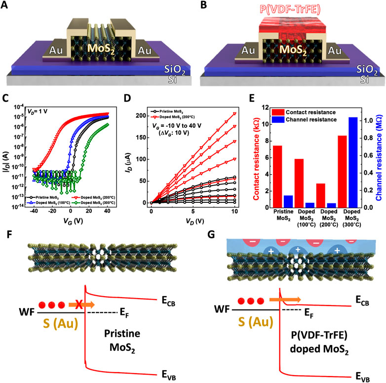
FIGURE 2. 3D schematic diagram of the (A) pristine and (B) P(VDF-TrFE)-doped MoS2 FET. (C) Transfer curves of the pristine MoS2 FET and the P(VDF-TrFE)-doped MoS2 FETs (100, 200, and 300°C). (D) Output curves of the pristine MoS2 FET and P(VDF-TrFE)-doped MoS2 FET (200°C). (C) Contact resistance and channel resistance of the pristine MoS2 FET and the P (VDF-TrFE)-doped MoS2 FETs (100, 200, and 300°C) extracted by the G-function method. (F) Energy band diagram of the pristine MoS2 FET. (G) Energy band diagram of the P(VDF-TrFE)-doped MoS2 FETs.
The electrical parameters were extracted to investigate the n-type doping effect of P(VDF-TrFE) induced on MoS2 FETs. The uniform n-type doping effects of the proposed approach were observed in terms of field effect mobility, on-current, and negatively shifted threshold voltage with 8 different MoS2 FETs. Figure 3A presents the average and maximum field effect mobility of pristine MoS2 FETs and P(VDF-TrFE)-doped MoS2 FETs. The average field effect mobility of 8 MoS2 FETs was extracted as a histogram and an error bar of standard error was added. In this work, the transfer curve of 8 MoS2 FETs for extracting electrical parameters was reported in Supplementary Figure S2. The electrical characteristics of MoS2 FETs are significantly impacted by various process factors. Chemical vapor deposition (CVD) and mechanical exfoliation with two common synthesis methods influenced the quality of MoS2 due to process variations (Kim et al., 2014, 2016; Choi et al., 2022). In addition, the contact resistance between the electrodes and channel of MoS2 FETs is changed based on the deposition method for metal, annealing temperature, and metal/MoS2 interface, resulting in variations in carrier mobility. Also, the performance of MoS2 FET is affected by the photolithography conditions that affected the surface morphology and quality of MoS2 (Plechinger et al., 2014; Wang et al., 2019; Yang et al., 2021). The average field effect mobility of the 8 pristine MoS2 FETs was 12.4 cm2 V−1s–1 and increased slightly to 12.5 cm2 V−1s–1 when the P(VDF-TrFE) annealing temperature was 100°C. The average field mobility of MoS2 FETs in the optimized P(VDF-TrFE) annealing (200°C) process was 15.1 cm2 V−1s–1. On the other hand, the field effect mobility of P(VDF-TrFE)-doped MoS2 FETs (300°C) was 6.7 cm2 V−1s–1, which is lower than pristine MoS2 FET. In addition, the MoS2 FET with the highest mobility was 26.9 cm2 V−1s–1 for the pristine sample, while it was 34.4 cm2 V−1s–1 under optimized annealing conditions. Also, the negative shifts in threshold voltage were observed at n-type doped MoS2 FETs. The dipole effect of top P(VDF-TrFE) region induces the conduction band and Fermi level of MoS2 closer. The downward energy band promotes rapid inversion due to enhanced electron tunneling, resulting in the threshold voltage shifting negatively. Supplementary Figure S3 shows the threshold voltages of pristine MoS2 FET and P(VDF-TrFE)-doped MoS2 FETs. The pristine MoS2 FET has a threshold voltage of 16.7 V. The P(VDF-TrFE)-doped MoS2 FET (100°C) has a negatively shifted threshold voltage of 9.8 V due to relatively weak n-type doping effect from the large fraction of non-polar α-phase P(VDF-TrFE). The P(VDF-TrFE)-doped MoS2 FET (200°C) under the optimized conditions with strong n-type doping effect had −8.9 V of threshold voltage due to the enlarged fraction of the polar ß phase P(VDF-TrFE). However, the threshold voltage of P(VDF-TrFE)-doped MoS2 FET (300°C) was shifted in the positive gate voltage direction (Vth = 30.6 V). This phenomenon is related with the Mo-O bonds generated in MoS2 during the high-temperature annealing. The Mo-O bonding created by adsorbed oxygen and water molecules causes a p-type doping effect in MoS2 (Wei et al., 2014). As a result, the n-type doping effect on P(VDF-TrFE)-doped MoS2 FET (300°C) was reduced owing to the Mo-O bonding induced p-type doping effect. Statistical analysis of 8 P(VDF-TrFE)-doped MoS2 FETs (200°C) was performed to investigate the uniformity of the P(VDF-TrFE) doping effect. The field effect mobility of the P(VDF-TrFE)-doped MoS2 FETs (200°C) increased by an average of 132% compared to the pristine MoS2 FET (Figure 3B). Figure 3C shows the enhancement ratio of on-current with the P(VDF-TrFE)-doped MoS2 FETs (200°C) compared to the pristine MoS2 FET. The n-type doping effect of P(VDF-TrFE) on MoS2 FETs increased the on-current of the 8 devices by an average of 201.8%. Supplementary Figure S4 represents the output curves of 8 P(VDF-TrFE)-doped MoS2 FETs (200°C). As shown in Supplementary Figure S4, 8P (VDF-TrFE)-doped MoS2 FETs (200°C) achieved increased drain current compared to pristine MoS2 FETs. In addition, the average threshold voltage of 19.6 V has been shifted negatively (Figure 3D).
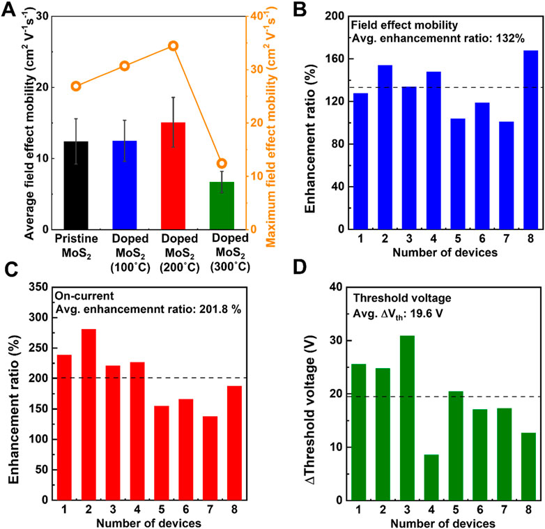
FIGURE 3. Electrical parameters of the pristine MoS2 FET and the P(VDF-TrFE)-doped MoS2 FETs (100 200, and 300°C) (A) Average and maximum field-effect mobilities. The enhancement ratio of 8 different P(VDF-TrFE)-doped MoS2 FETs (200°C): (B) Field-effect mobility, (C) on-current, and (D) changes in the threshold voltage values compared to pristine devices.
We further validated the robust n-type doping effect of the proposed method through a thermal stability characterization. Figure 4A shows a 3D schematic description of the experimental environment with P(VDF-TrFE)-doped MoS2 FET (200°C). More specifically, the P(VDF-TrFE)-doped MoS2 FET (200°C) was placed in the hot-chuck mounted probe station chamber. The temperature was increased from room temperature (RT, 20°C) to 100°C and maintained for 1 h. After 1 h, the chamber was naturally cooled to 20°C. The electrical characterization of the device was measured during the whole thermal sequence at specific points. Figure 4B displays the threshold voltage variation of the P(VDF-TrFE)-doped MoS2 FETs (200°C) during the heating-up condition range of 20–100°C. The threshold voltage before the thermal stability test was measured to 17.4 V (at 20°C condition). While increasing the thermal condition of the chamber up to 100°C, the threshold voltage values were varied with the lowest value of 14.6 V (at 60°C) and the highest value of 18.4 V (at 100°C). The average threshold voltage measured during the 5 steps is 16.9 V, which represents a negligible difference of 0.5 V compared to the pristine value (17.4 V). Furthermore, the above-mentioned stable threshold voltage retention was demonstrated even under continuous thermal conditions (100°C for 1 h). As shown in Figure 4C, the threshold voltage values measured at each of the 10 min cycles were almost maintained without any sudden degradation or fluctuation, which proves the good thermal stability of the proposed device at 100°C environments. Figure 4D shows the comparison of transfer curves before and after the thermal stability test. Compared to the initial characteristics, only slight changes were observed with an increase in off-current and on-current with the values of 14.7 nA and 28.9 µA.
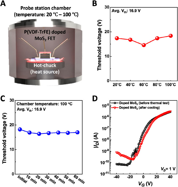
FIGURE 4. (A) 3D schematic description of the thermal stability characterization environment. Threshold voltage change according to the experimental conditions: (B) during the chamber temperature increasement from 20 to 100°C, (C) continuous 100 °C environment condition for 1 h. (D) Transfer curves of the P(VDF-TrFE)-doped MoS2 FET (200°C) before and after the thermal stability characterization.
3.2 Effect of phase transition on n-type doping states
Next, to understand the optimized n-type doping condition (200°C annealing temperature), we investigated the change in the dopant P(VDF-TrFE) film according to the annealing variation. As discussed previously, the main mechanism of n-type doping on MoS2 by P(VDF-TrFE) is based on the dipole moment in the dopant film. Depending on the molecular arrangement, P(VDF-TrFE) has three different crystalline structures: α, β, and γ phases. Among them, the ß and γ phases exhibited polar dipole moments owing to their geometric configuration, as shown in Figure 5A (Shepelin et al., 2019; Arrigoni et al., 2020). The crystalline phases of P(VDF-TrFE) mentioned above can be obtained through a sequential melting and recrystallization process (García-Gutiérrez et al., 2013; Arifin and Ruan, 2018). The non-polar α phase, however, is the most thermodynamically stable form, so the P(VDF-TrFE) polymer crystallizes preferentially into it during melting and recrystallization. Based on this phenomenon, it was predicted that different ratios of the polar phases (β and γ) and non-polar (α) phase would be formed according to the annealing conditions. As a result of the phase variation, the higher polar phase ratio leads to strong n-type doping effects on MoS2 FETs observed during electrical characterization.
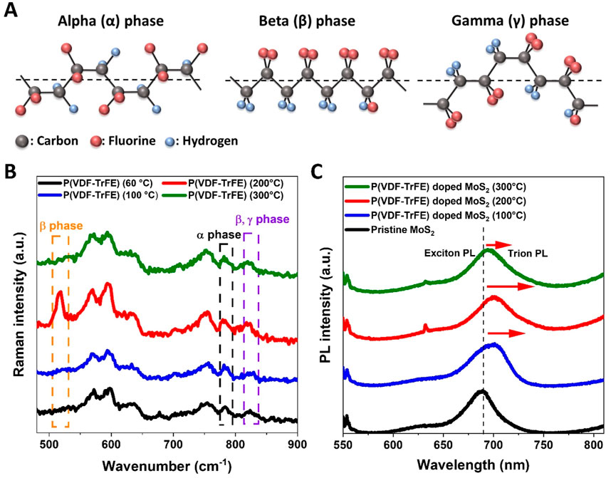
FIGURE 5. (A) Schematic description of different crystalline phases of P(VDF-TrFE) polymer with geometric configurations. (B) Raman spectra of P(VDF-TrFE) films varied with different annealing conditions. Specific peak ranges for α, β, and γ phases are highlighted with black, orange, and violet color dashed boxes. (C) PL spectra of MoS2 flakes according to n-type doping conditions. The red arrows indicate the direction of the peak shift compared to the pristine sample.
Raman spectroscopy was performed to observe the crystalline phases of the P(VDF-TrFE) films varied with annealing conditions (Figure 5B). Specific peaks according to the α, β, and γ phases of P(VDF-TrFE) were identified. The non-polar α phase appeared in all samples with the peak range at 775 cm−1 to 795 cm−1 (black dashed box) (Riosbaas et al., 2014). The peak indicated a high polar ß phase (510 cm−1, orange dashed box) (Viswanath and Yoshimura, 2019) was observed only in the sample (annealed at 200°C), which exhibited the most n-doped characteristic. Furthermore, the intensity of peaks at 810 cm−1 to 840 cm−1 (violet dashed box, mixed phases of polar ß and γ) (Singh et al., 2014) tended to increase in the order of efficiency of the n-type doping effect in electrical characterization results (Figures 2C, 3A). The most n-doped 200°C annealed sample exhibited a clear polar ß phase. The intensity ratio of α phase/β and γ mixed phase were reduced after 300°C annealing. The polar phase increase according to the recrystallizing condition in P(VDF-TrFE) film was cross-validated through contact angle measurements. As reported in previous studies, the enrichment of crystallization domains on the surface of the PVDF-based polymer films also can promote the hydrophilicity (low water contact angle) (Chen and Hong, 2002; Zhao et al., 2012). The increased polar crystalline phases enhance the surface polarity of the films, and results in the reduced water contact angle. As shown in Supplementary Figure S6, the water contact angle change according to the annealing condition is consistent with the ß phase intensity ratio change from Raman analysis. The contact angle showed the lowest value at 200°C annealing condition where the ß phase peak intensity and n-type doping effect on MoS2 FET were maximum, and slightly increased at 300°C when the n-type doping effect was weakened. The above results are well-matched with the relationship between polar phase formation and n-type doping efficiency. PL characterization supports the variation of n-type doping effects according to the dopant film phases. As shown in Figure 5C, the PL emission peaks were red-shifted for all doped samples, representing increased trion-related emissions in n-doped states. Nevertheless, the shifted values varied with the n-type doping conditions. The peak shifts were 10, 12, and 6 nm for the 100, 200, and 300°C annealed samples, which agree well with the n-type doping efficiency trends discussed above. Through the above characterization, it was confirmed that the P(VDF-TrFE) dopant film provides a strong n-type doping effect on MoS2 FETs by forming polar crystalline phases.
4 Conclusion
In summary, we proposed the dipole-induced n-type doping approach for MoS2 FET with the P(VDF-TrFE) polymer dopant. The n-type doping effects on MoS2 FETs were varied with the phase transition of the top P(VDF-TrFE) region by controlling recrystallization conditions. The controllable doping states according to the phase transition of P(VDF-TrFE) layers were investigated with Raman and PL spectroscopies. The increased polar phases of P(VDF-TrFE) dopant layer provide the enhanced n-type operation to MoS2 FET by reducing the contact resistance. At the optimized condition, the field effect mobility, and the on-current values of the P(VDF-TrFE) doped MoS2 FET were achieved 34.4 cm2 V−1s–1 and 21 μA, respectively. The n-type doping effects observed at 8 different MoS2 FETs and operation in a harsh environment imply that the proposed doping methods stable and reliable. We hope that the proposed approach could be utilized for further applications in the field of 2D semiconductor-based transistors and related research fields.
Data availability statement
The raw data supporting the conclusion of this article will be made available by the authors, without undue reservation.
Author contributions
DHL, TP, and HY designed the conception of the article, analysis of data, and work on manuscript preparation. DHL and TP performed experiments and collect the data. TJ, YJ, JP, NJ, and UW contribute d to the interpretation of data and analysis of results. All authors listed have made a substantial, direct, and intellectual contribution to the work. DHL, and TP equally contribute this work.
Funding
This work was supported by the research projection “Development of two-dimensional material heterojunction type spin transistor device to improve power efficiency of electronic components (202203370001),” Hyundai Motor Company. This work was supported by the Gachon University research fund of 2022 (GCU- 202206060001).
Conflict of interest
Authors TJ, YJ, JP, NJ, and UW were employed by the company Hyundai Motor Group.
The remaining authors declare that the research was conducted in the absence of any commercial or financial relationships that could be construed as a potential conflict of interest.
The authors declare that this study received funding from Hyundai Motor Group. The funder had the following involvement in the study: the study design and data analysis.
Publisher’s note
All claims expressed in this article are solely those of the authors and do not necessarily represent those of their affiliated organizations, or those of the publisher, the editors and the reviewers. Any product that may be evaluated in this article, or claim that may be made by its manufacturer, is not guaranteed or endorsed by the publisher.
Supplementary material
The Supplementary Material for this article can be found online at: https://www.frontiersin.org/articles/10.3389/fmats.2023.1139954/full#supplementary-material
References
Arifin, D. E. S., and Ruan, J. J. (2018). Study on the curie transition of P (VDF-TrFE) copolymer. IOP Conf. Ser. Mater. Sci. Eng. 299, 012056. doi:10.1088/1757-899X/299/1/012056
Arrigoni, A., Brambilla, L., Bertarelli, C., Serra, G., Tommasini, M., and Castiglioni, C. (2020). P (VDF-TrFE) nanofibers: Structure of the ferroelectric and paraelectric phases through IR and Raman spectroscopies. RSC Adv. 10, 37779–37796. doi:10.1039/d0ra05478j
Brill, A. R., Kafri, A., Mohapatra, P. K., Ismach, A., de Ruiter, G., and Koren, E. (2021). Modulating the optoelectronic properties of MoS2 by highly oriented dipole-generating monolayers. ACS Appl. Mat. Inter. 13, 32590–32597. doi:10.1021/acsami.1c09035
Chakraborty, B., Bera, A., Muthu, D. V. S., Bhowmick, S., Waghmare, U., and Sood, A. K. (2012). Symmetry-dependent phonon renormalization in monolayer MoS2 transistor. Phys. Rev. B 85, 161403. doi:10.1103/physrevb.85.161403
Chen, N., and Hong, L. (2002). Surface phase morphology and composition of the casting films of PVDF–PVP blend. Polym. Guildf. 43, 1429–1436. doi:10.1016/s0032-3861(01)00671-1
Choi, M., Bae, S.-R., Hu, L., Hoang, A. T., Kim, S. Y., and Ahn, J.-H. (2020). Full-color active-matrix organic light-emitting diode display on human skin based on a large-area MoS2 backplane. Sci. Adv. 6, eabb5898. doi:10.1126/sciadv.abb5898
Choi, M., Lee, J. W., and Lee, H. S. (2022). Optical and electrical characterizations of volatile doping effect originated from bilayer photoresist process in MoS2 field-effect transistors. J. Korean Phys. Soc. 81, 317–324. doi:10.1007/s40042-022-00525-8
Choi, Y.-Y., Yun, T. G., Qaiser, N., Paik, H., Roh, H. S., Hong, J., et al. (2015). Vertically aligned P (VDF-TrFE) core-shell structures on flexible pillar arrays. Sci. Rep. 5, 10728. doi:10.1038/srep10728
Gant, P., Huang, P., de Lara, D. P., Guo, D., Frisenda, R., and Castellanos-Gomez, A. (2019). A strain tunable single-layer MoS2 photodetector. Mat. Today 27, 8–13. doi:10.1016/j.mattod.2019.04.019
García-Gutiérrez, M.-C., Linares, A., Martín-Fabiani, I., Hernández, J. J., Soccio, M., Rueda, D. R., et al. (2013). Understanding crystallization features of P (VDF-TrFE) copolymers under confinement to optimize ferroelectricity in nanostructures. Nanoscale 5, 6006–6012. doi:10.1039/c3nr00516j
Hwangbo, S., Hu, L., Hoang, A. T., Choi, J. Y., and Ahn, J.-H. (2022). Wafer-scale monolithic integration of full-colour micro-LED display using MoS2 transistor. Nat. Nanotechnol. 17, 500–506. doi:10.1038/s41565-022-01102-7
Jiang, L., Liu, J., Shi, Y., Zhu, D., Zhang, H., Hu, Y., et al. (2019). Realizing low-voltage operating crystalline monolayer organic field-effect transistors with a low contact resistance. J. Mat. Chem. C 7, 3436–3442. doi:10.1039/c9tc00443b
Kang, D., Kim, M., Shim, J., Jeon, J., Park, H., Jung, W., et al. (2015). High-performance transition metal dichalcogenide photodetectors enhanced by self-assembled monolayer doping. Adv. Funct. Mat. 25, 4219–4227. doi:10.1002/adfm.201501170
Kim, I. S., Sangwan, V. K., Jariwala, D., Wood, J. D., Park, S., Chen, K.-S., et al. (2014). Influence of stoichiometry on the optical and electrical properties of chemical vapor deposition derived MoS2. ACS Nano 8, 10551–10558. doi:10.1021/nn503988x
Kim, T.-Y., Amani, M., Ahn, G. H., Song, Y., Javey, A., Chung, S., et al. (2016). Electrical properties of synthesized large-area MoS2 field-effect transistors fabricated with inkjet-printed contacts. ACS Nano 10, 2819–2826. doi:10.1021/acsnano.5b07942
Kim, T., Fan, S., Lee, S., Joo, M.-K., and Lee, Y. H. (2020). High-mobility junction field-effect transistor via graphene/MoS2 heterointerface. Sci. Rep. 10, 13101–13108. doi:10.1038/s41598-020-70038-6
Krishnan, K. N., Sreedharan, A., Sagar, S., Thomas Manamel, L., Mukherjee, A., and Das, B. C. (2021). Self-Powered broadband photodetection of copper phthalocyanine by enhancing photogating effect with monolayer MoS2 flakes. Appl. Surf. Sci. 568, 150818. doi:10.1016/j.apsusc.2021.150818
Kumar, R., Zheng, W., Liu, X., Zhang, J., and Kumar, M. (2020). MoS2-based nanomaterials for room-temperature gas sensors. Adv. Mat. Technol. 5, 1901062. doi:10.1002/admt.201901062
Lee, G.-H., Yu, Y.-J., Cui, X., Petrone, N., Lee, C.-H., Choi, M. S., et al. (2013). Flexible and transparent MoS2 field-effect transistors on hexagonal boron nitride-graphene heterostructures. ACS Nano 7, 7931–7936. doi:10.1021/nn402954e
Li, Y., Xu, C.-Y., Hu, P., and Zhen, L. (2013). Carrier control of MoS2 nanoflakes by functional self-assembled monolayers. ACS Nano 7, 7795–7804. doi:10.1021/nn402682j
Lin, C.-Y., Simbulan, K. B., Hong, C.-J., Li, K.-S., Zhong, Y.-L., Su, Y.-K., et al. (2020). Polarity-controllable MoS2 transistor for adjustable complementary logic inverter applications. Nanoscale Horiz. 5, 163–170. doi:10.1039/c9nh00275h
Liu, C., Minari, T., Xu, Y., Yang, B., Chen, H.-X., Ke, Q., et al. (2015). Direct and quantitative understanding of the non-Ohmic contact resistance in organic and oxide thin-film transistors. Org. Electron. 27, 253–258. doi:10.1016/j.orgel.2015.09.024
Maity, N., Mandal, A., and Nandi, A. K. (2017). High dielectric poly (vinylidene fluoride) nanocomposite films with MoS2 using polyaniline interlinker via interfacial interaction. J. Mat. Chem. C 5, 12121–12133. doi:10.1039/c7tc03593d
Manamel, L. T., Mukherjee, A., and Das, B. C. (2020). Two-dimensional nanohybrid of MoS2 and Rose Bengal: Facile solution growth and band structure probing. Appl. Surf. Sci. 530, 147063. doi:10.1016/j.apsusc.2020.147063
McClellan, C. J., Yalon, E., Smithe, K. K. H., Suryavanshi, S., and Pop, E. (2021). High current density in monolayer MoS2 doped by AlOX. ACS Nano 15, 1587–1596. doi:10.1021/acsnano.0c09078
Meng, N., Ren, X., Zhu, X., Wu, J., Yang, B., Gao, F., et al. (2020). Multiscale understanding of electric polarization in poly (vinylidene fluoride)-based ferroelectric polymers. J. Mat. Chem. C 8, 16436–16442. doi:10.1039/d0tc04310a
Miller, B., Parzinger, E., Vernickel, A., Holleitner, A. W., and Wurstbauer, U. (2015). Photogating of mono-and few-layer MoS2. Appl. Phys. Lett. 106, 122103. doi:10.1063/1.4916517
Nickel, N. H., Lengsfeld, P., and Sieber, I. (2000). Raman spectroscopy of heavily doped polycrystalline silicon thin films. Phys. Rev. B 61, 15558–15561. doi:10.1103/physrevb.61.15558
Pak, S., Jang, A.-R., Lee, J., Hong, J., Giraud, P., Lee, S., et al. (2019). Surface functionalization-induced photoresponse characteristics of monolayer MoS2 for fast flexible photodetectors. Nanoscale 11, 4726–4734. doi:10.1039/c8nr07655c
Pham, T., Li, G., Bekyarova, E., Itkis, M. E., and Mulchandani, A. (2019). MoS2-based optoelectronic gas sensor with sub-parts-per-billion limit of NO2 gas detection. ACS Nano 13, 3196–3205. doi:10.1021/acsnano.8b08778
Plechinger, G., Mann, J., Preciado, E., Barroso, D., Nguyen, A., Eroms, J., et al. (2014). A direct comparison of CVD-grown and exfoliated MoS2 using optical spectroscopy. Semicond. Sci. Technol. 29, 064008. doi:10.1088/0268-1242/29/6/064008
Riosbaas, M. T., Loh, K. J., O’Bryan, G., and Loyola, B. R. (2014). “In situ phase change characterization of PVDF thin films using Raman spectroscopy,” in Sensors and Smart Structures Technologies for Civil, Mechanical, and Aerospace Systems 2014, Bellingham, 21 April 2014 (United States: SPIE), 235–245.
Sahoo, M. K., and Kale, P. G. (2019). Micro-Raman study of growth parameter restraint for silicon nanowire synthesis using MACE. Superlattices Microstruct. 135, 106289. doi:10.1016/j.spmi.2019.106289
Samy, O., Zeng, S., Birowosuto, M. D., and el Moutaouakil, A. (2021). A review on MoS2 properties, synthesis, sensing applications and challenges. Crystals 11, 355. doi:10.3390/cryst11040355
Schauble, K., Zakhidov, D., Yalon, E., Deshmukh, S., Grady, R. W., Cooley, K. A., et al. (2020). Uncovering the effects of metal contacts on monolayer MoS2. ACS Nano 14, 14798–14808. doi:10.1021/acsnano.0c03515
Shen, T., Li, F., Xu, L., Zhang, Z., Qiu, F., Li, Z., et al. (2020). High mobility monolayer MoS2 transistors and its charge transport behaviour under E-beam irradiation. J. Mat. Sci. 55, 14315–14325. doi:10.1007/s10853-020-04977-w
Shepelin, N. A., Glushenkov, A. M., Lussini, V. C., Fox, P. J., Dicinoski, G. W., Shapter, J. G., et al. (2019). New developments in composites, copolymer technologies and processing techniques for flexible fluoropolymer piezoelectric generators for efficient energy harvesting. Energy Environ. Sci. 12, 1143–1176. doi:10.1039/c8ee03006e
Singh, P., Borkar, H., Singh, B. P., Singh, V. N., and Kumar, A. (2014). Ferroelectric polymer-ceramic composite thick films for energy storage applications. AIP Adv. 4, 087117. doi:10.1063/1.4892961
Tanwar, M., Bansal, L., Rani, C., Rani, S., Kandpal, S., Ghosh, T., et al. (2022). Fano-type wavelength-dependent asymmetric Raman line shapes from MoS2 nanoflakes. ACS Phys. Chem. Au 2, 417–422. doi:10.1021/acsphyschemau.2c00021
Viswanath, P., and Yoshimura, M. (2019). Light-induced reversible phase transition in polyvinylidene fluoride-based nanocomposites. SN Appl. Sci. 1, 1519–9. doi:10.1007/s42452-019-1564-3
Wang, L., Chen, L., Wong, S. L., Huang, X., Liao, W., Zhu, C., et al. (2019). Electronic devices and circuits based on wafer-scale polycrystalline monolayer MoS2 by chemical vapor deposition. Adv. Electron. Mat. 5, 1900393. doi:10.1002/aelm.201900393
Wang, S., Zeng, X., Zhou, Y., Lu, J., Hu, Y., Wang, W., et al. (2022). High-performance MoS2 complementary inverter prepared by oxygen plasma doping. ACS Appl. Electron. Mat. 4, 955–963. doi:10.1021/acsaelm.1c01070
Wang, Y., Gali, S. M., Slassi, A., Beljonne, D., and Samorì, P. (2020). Collective dipole-dominated doping of monolayer MoS2: Orientation and magnitude control via the supramolecular approach. Adv. Funct. Mat. 30, 2002846. doi:10.1002/adfm.202002846
Wei, X., Yu, Z., Hu, F., Cheng, Y., Yu, L., Wang, X., et al. (2014). Mo-O bond doping and related-defect assisted enhancement of photoluminescence in monolayer MoS2. AIP Adv. 4, 123004. doi:10.1063/1.4897522
Woo, W. J., Lee, E. K., Yoo, H., and Kim, T. (2021a). Unprecedentedly uniform, reliable, and centimeter-scale molybdenum disulfide negative differential resistance photodetectors. ACS Appl. Mat. Inter. 13, 25072–25081. doi:10.1021/acsami.1c02880
Woo, W. J., Seo, S., Nam, T., Kim, Y., Kim, D., Song, J.-G., et al. (2021b). MoS2 doping by atomic layer deposition of high-k dielectrics using alcohol as process oxidants. Appl. Surf. Sci. 541, 148504. doi:10.1016/j.apsusc.2020.148504
Yang, H., Cai, S., Zhang, Y., Wu, D., and Fang, X. (2021). Enhanced electrical properties of lithography-free fabricated MoS2 field effect transistors with chromium contacts. J. Phys. Chem. Lett. 12, 2705–2711. doi:10.1021/acs.jpclett.1c00231
Yoo, H., Hong, S., On, S., Ahn, H., Lee, H.-K., Hong, Y. K., et al. (2018). Chemical doping effects in multilayer MoS2 and its application in complementary inverter. ACS Appl. Mat. Inter. 10, 23270–23276. doi:10.1021/acsami.8b08773
Zhao, X., Cheng, J., Zhang, J., Chen, S., and Wang, X. (2012). Crystallization behavior of PVDF/PMMA blends prepared by in situ polymerization from DMF and ethanol. J. Mat. Sci. 47, 3720–3728. doi:10.1007/s10853-011-6221-1
Keywords: transition-metal dichalcogenides, molybdenum disulfide, polar polymer, dipole moment effects, field effect transistors
Citation: Lee DH, Park T, Jeong T, Jung Y, Park J, Joo N, Won U and Yoo H (2023) Dipole doping effect in MoS2 field effect transistors based on phase transition of ferroelectric polymer dopant. Front. Mater. 10:1139954. doi: 10.3389/fmats.2023.1139954
Received: 08 January 2023; Accepted: 20 March 2023;
Published: 04 April 2023.
Edited by:
Li Tao, Beijing Institute of Technology, ChinaReviewed by:
Abu Zayed M. Saliqur Rahman, Intelligent Actuator Incorporation, United StatesBikas C. Das, Indian Institute of Science Education and Research, Thiruvananthapuram, India
Copyright © 2023 Lee, Park, Jeong, Jung, Park, Joo, Won and Yoo. This is an open-access article distributed under the terms of the Creative Commons Attribution License (CC BY). The use, distribution or reproduction in other forums is permitted, provided the original author(s) and the copyright owner(s) are credited and that the original publication in this journal is cited, in accordance with accepted academic practice. No use, distribution or reproduction is permitted which does not comply with these terms.
*Correspondence: Hocheon Yoo, aHlvb0BnYWNob24uYWMua3I=