 Zewen Tan1,2,3
 Zheng Li
- 1School of Physics and Optoelectronic Engineering, Ludong University, Yantai, China
- 2School of Integrated Circuits, Ludong University, Yantai, China
- 3Engineering Research Center of Photodetector Special Chip in Universities of Shandong, Ludong University, Yantai, China
- 4School for Optoelectronic Engineering, Zaozhuang University, Zaozhuang, Shandong, China
- 5Institute of Microelectronics, Chinese Academy of Sciences (IMECAS), Beijing, China
- 6School of Physics Engineering, Qufu Normal University, Qufu, Shandong, China
Among the 3D electrode Si detectors for high energy particle and X-ray detection, the traditional 3D-Trench electrode Si detector is a semiconductor detector that is widely used and discussed. Aiming at removing the shortcomings of the traditional 3D-Trench electrode Si detectors such as uneven electric field distribution, asymmetric electric potential, and the existence of some dead zone, we propose a new type 3D-Spherical Electrode Detectors and carry out extensive and systematic studies of their physical properties. We simulated detector electric field, electric potential, electron concentration distribution, full depletion voltage, leakage current, capacitance, the incident particle induced transient current and the weighting field. We systematically studied and analyzed detector’s electrical characteristics. By comparing with the traditional 3D-Trench electrode Si detectors, the new detector structure has more uniform electric field and potential, and less depletion voltage, leakage current and capacitance.
Introduction
At present, with the advancement of society and the development of science and technology, the application of semiconductor materials has become an indispensable part of life (Meng., 2009). Detectors based on semiconductor materials have also emerged (X.Meng., 2004). Traditional detector technology is becoming more and more mature. Among a large number of semiconductor detectors, silicon detectors are widely used in aerospace (W.Wei and AuthorAnonymous, 2005), astrophysics (Guo., 2013), high energy physics (Ou., 1998), nuclear medicine (Qin., 2007), national security (W.Wei and AuthorAnonymous, 2005), and other fields due to their superior performance and mature advanced technology.
Common types of silicon detectors mainly include silicon microstrip detectors, silicon pixel detectors, silicon drift detectors, 3D-column electrode silicon detectors, and 3D-Trench electrode Si detectors (Liu., 2018), (Tang., 2017). With the evolution and development of various types of semiconductor detectors, from two-dimensional to three-dimensional, the structure and performance of the detectors are gradually improving and perfecting.
For 3D electrode Si detectors, there are shortcomings in the detector structures (Liao., 2019). For example, for traditional 3D-Trench electrode Si detectors, it is needed to ensure that during and after etching, the detectors main body does not fall off the substrate. The trench electrode cannot completely penetrate the entire silicon substrate and can only be etched to about 90% of the depth of the silicon substrate. Therefore, the first shortcoming of the traditional 3D-Trench electrode Si detectors is the existence of a dead zone in the un-etched region. During the processing and manufacturing of a 3D-Trench electrode Si detectors, the Si wafer cannot be completely etched through, that is, a certain thickness will remain on the wafer as a substrate to ensure the mechanical stability of the detector structure unit or array (Betta et al., 2010). The dead zone is a weak or zero electric field region that exists in the un-etched detector part. If the dead zone occupies a large portion of the detector volume, the detector electrical characteristics will be poor, such as uneven electric field distribution and the existence of a low electric field region, affecting the detector charge collection efficiency (Lu., 2020).
In view of the above-mentioned shortcomings of traditional 3D-Trench electrode Si detectors, a new type of hemispherical shell electrode silicon detector has been proposed in recent years (Liu et al., 2020a). The structural model of this detector can indeed solve the problem of the dead zone of traditional 3D-Trench electrode Si detectors. As a detector unit, the detector performance of the spherical detector is very prominent, which can be verified by simulations, But ideal spherical structure will be relatively difficult to realize in real processing and production.
In this article, a Practical Novel 3D-Spherical Electrode Detector is proposed and its physical properties are systematically studied. The spherical electrode in the novel detectors is realized through laser drillings of Si wafer (Zhi-Ming et al., 2017). We will use ion diffusion technology. Respective ions will be thermally diffused into the Si through the walls of drilled trenches, an effective spherical electrode can be practically formed.
Figure 1 shows the cross-section of the new detector scheme. Rings of trenches with width wi, depth yi, and radius xi (i = 1,. N) will be drilled by a laser through the Si wafer. To form an effective spherical electrode, we must have the following relationship between x, y, and R:
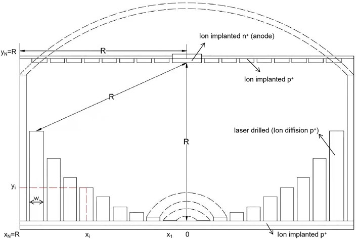
FIGURE 1. Cross-section view with the same distance between anode and cathode.
For simplicity, we keep the trench width at a constant w = w0. The number of drilled trenches can be chosen according to the size of the detector and laser drilling limitations (e.g. minimum drilling width wm, maximum drilling time and power, etc.)
After drilling, trench walls will be ion diffused to form a junction with the Si wafer bulk (in this case, we chose n-type Si bulk, the ion diffusion is p-type, i.e.boron).
To connect all trenches, the entire bottom side of the wafer will be ion-implanted with boron ions to form a p+ layer that connects all p+ trenches.
To make the field distribution on the top surface more uniform, we make ion-implant rings (p+) as field guard rings.
Modeling of the Practical Novel 3D-Spherical Electrode Detectors
The approximate model of the detector is shown in Figure 2. There is a 200 μm × 200 μm × 100 μm cubic column semiconductor substrate, which is lightly doped with N-type, and the doping concentration is 1 × 10¹²/cm3. On the top layer, there is an n+-implanted area (radius = 17.5 μm) in the center covered by an aluminum layer to form the collection anode electrode. The areas between anode and field guard rings are SiO2 layers. These field guard rings are heavily doped p+ (1 × 10¹⁸/cm3) rings. The back side is uniformly heavily doped with p+ (1 × 10¹⁸/cm3). The anode is heavily doped with n+ (1 × 10¹⁸/cm3). The doping depths of all implanted layers are 1 μm, as shown in Figure 3. The cathode is composed of ten laser-drilled rings (in the X-axis cross-section they look like columns). The laser-drilled rings are heavily doped with P-type through ion diffusion, and the doping concentration is 1 × 10¹⁹/cm3. The bottom is covered by an aluminum layer to form a whole cathode electrode. The thickness of the aluminum electrode contact layer on the upper and lower surfaces is 1 μm, and the thickness of the SiO2 on the upper and lower surfaces is 0.5 μm.
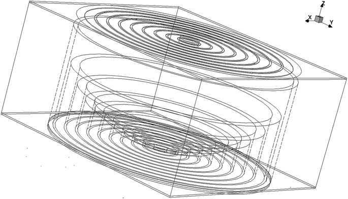
FIGURE 2. 3D structure of Practical Novel 3D-Spherical-Electrode Detectors structure.
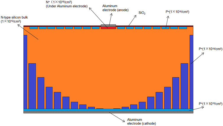
FIGURE 3. The sectional view of Practical Novel 3D-Spherical-Electrode Detectors structure.
The structure size and internal structure are calculated according to Eq. 1. For a given pitch p, width w, and gap g = βp for the drilled trenches, since d = R, we have:
Where xi represents the distance from the center coordinate of the etched column to the origin, yi represents the height of the etched column, i represents the number of the drilled trenches, N represents the number of trenches,
Where:
We have:
In our simulations, we choose R = 100 μm, β = 0.8, p = 10 μm, W = 8, and N = 10. Y10 = 0.9*R.
In this article, the junction of the 3D-Spherical-Electrode detectors is at the outer spherical shell electrode. Due to the spherical symmetry of our new detector structure, we can reduce the problem to a one-dimensional one with only r, and write the Poisson equation as the following:
with boundary conditions:
The electric field is:
and the electric potential in a single cell is:
When
We get the full depleted voltage:
Electrical characteristics results
3D simulation and electric field distribution of Practical Novel 3D-Spherical-Electrode Detectors
We used TCAD to simulate the 3D-Spherical electrode silicon detector unit (Zhou., 2013), with the SRH model, mobility model, and other common physical models in the simulation. The Poisson equation, electron continuity equation, and hole continuity equation are used as well (Zhu., 2011). Figure 4 shows the model of the new 3D spherical electrode structure used in our TCAD simulations, in which one can easily find out the parameters used for the simulation and one can clearly see the appearance and internal structure of the 3D spherical electrode silicon detector unit. The area of the aluminum electrode contact layer and the silicon dioxide protective layer are clearly shown. In addition to simulating a spherical electrode with a radius of 100 μm, we also simulated a 3D-Trench electrode Si detector of the same size (Ding, 2015), (Liu and Li, 2017). Through comparison, the superior electrical performance of this detector structure can be displayed more clearly and comprehensively.
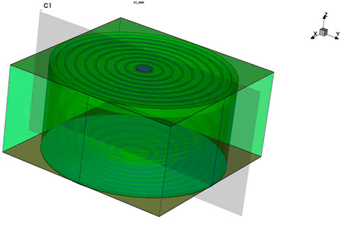
FIGURE 4. 3D simulation structure in the interface of TCAD simulation software.
We set up a two-dimensional cross-section at x = 0 to more clearly show the potential and electric field distribution inside the detector. Figure 5 shows the electric field distribution of Practical Novel 3D-Spherical-Electrode Detectors under different bias voltages. It can be seen that with the increase of the bias voltage, the low electric field area in the detector gradually becomes smaller. When the full depletion voltage is reached, the internal electric field reaches all parts of the detector, and the zero electric field area disappears. It can be inferred from the figure below that it is fully depleted at a voltage of about -3 V (full depletion voltage Vfd). In addition, we can clearly see that the electric field distribution in the depletion zone in the detector is extremely uniform, ensuring good charge collection in the entire effective detector body. The electric field lines are going through the top center anode electrode, with the direction pointing radially toward the spherical cathode electrode. This electric field distribution ensures the electrons induced by the incident particles drift toward the central collecting electrode in the electric field (Liu et al., 2017).
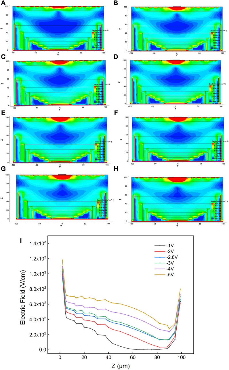
FIGURE 5. 2D electric field distribution of Practical Novel 3D-Spherical-Electrode Detectors under different voltages (A) -1V (B) -2V (C) -2.2V (D) -2.4V (E) -2.6V (F) -2.8V (G) -3V (H) -4V, and 1D cutline (I).
Figure 5I shows the electric field intensity curve inside the detector under different voltages (Li et al., 2021). It is along the cutline of y = 0 in Figure 5I. It can be seen more intuitively that as the bias voltage increases, the electric field intensity continues to increase, and fill the whole detector thickness.
Figure 6 shows the electric field distribution of a 3D-Trench electrode Si detector with the same size as Practical Novel 3D-Spherical-Electrode Detectors with a radius of 100 μm. It can be clearly seen by comparison that the electric field distribution is not as uniform as that in the Practical Novel 3D-Spherical Electrode Detector.
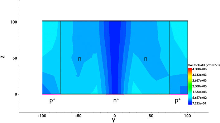
FIGURE 6. Electric field distribution of traditional 3D-Trench electrode Si detectors.
Electric potential distribution of Practical Novel 3D-Spherical-Electrode Detectors
Figure 7A shows the potential distribution of Practical Novel 3D-Spherical-Electrode Detectors (at v = -3 V at the cathode). It can be seen that the potential distribution of the structure is very symmetrical. To reversely bias the detector and to ensure the free electrons drifting to and being collected by the anode, the electric potential of the center anode on the upper surface is the highest (at 0 V).
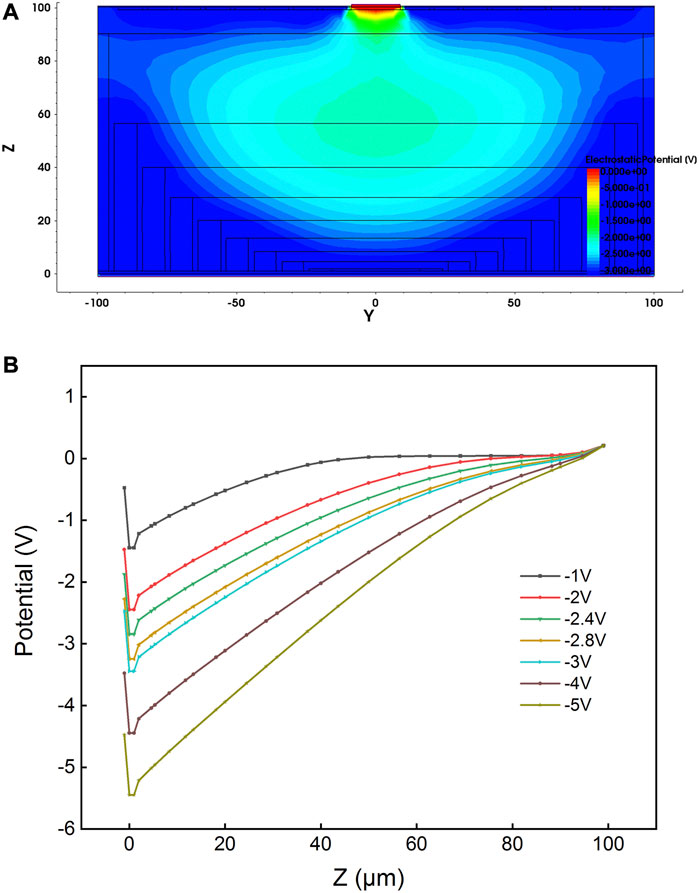
FIGURE 7. (A) 2D electric potential distribution and (B) internal electric potential curve at different voltages of Practical Novel 3D-Spherical-Electrode Detectors.
Figure 7B) shows the internal electric potential curves at different voltages applied to Practical Novel 3D-Spherical-Electrode Detectors on the cutlines at y = 0 (Liu et al., 2020b). These potential curves are almost linear. When the potential of the entire detector is not zero, it indicates that the detector is fully depleted. The bias voltage applied when the detector is fully depleted is the full depletion voltage (Tang, 2017). It can be seen from the figure that the depletion voltage is about -2.8 V. In addition, the slope of the potential curve increases with the increase of the bias voltage, that is, the intensity of the electric field increases with the increase of the bias voltage, which is a good verification of the relationship between the electric field and the bias voltage described above.
Figure 8 shows the electric potential distribution of a traditional 3D-Trench electrode Si detector. It can be seen that at Z = 15 μm, the electric potential distribution is obviously not as uniform.
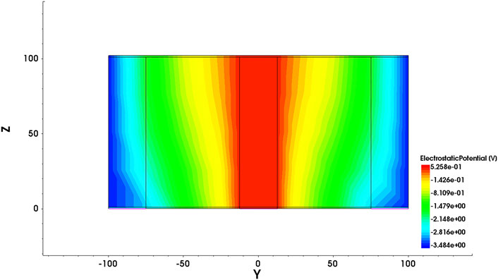
FIGURE 8. Electric potential distribution of 3D-Trench electrode Si detectors.
Full depletion voltage of Practical Novel 3D-Spherical-Electrode Detectors
In our Practical Novel 3D-Spherical-Electrode Detectors, the N-type silicon bulk has a doping concentration of 1×10¹²/cm3, so Neff = 1×10¹²/cm3. The detector thickness is chosen as 100 μm. According to Eq. 16, we can get a full depletion voltage Vfd ≈ -2.5 V, so the depletion voltage of our Practical Novel 3D-Spherical-Electrode Detectors should be around 2.5V, which is close to our previous value of -2.8 V obtained from simulations.
Figure 9A is the electron concentration curves obtained from simulations. The electron concentration in the depletion region decreases with the bias voltage (the depletion region of the detector continues to expand) until it reaches complete depletion (full depletion). It can be seen that when the voltage reaches -2.8 V, the electron concentration in the whole detector region is lower than the silicon substrate concentration of 1×10¹²/cm3. So we can conclude that the depletion voltage is -2.8 V, which is the same as what we obtained from electric field simulations. There is a certain difference between the results obtained by simulation and theoretical calculations because the theoretical value is under the premise of an ideal sphere without complicated boundary conditions.
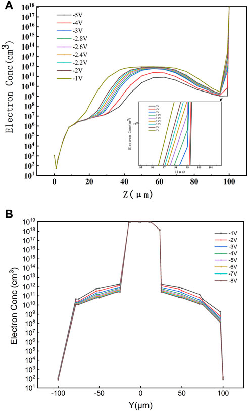
FIGURE 9. Electron concentration curve (log scale) v. s Bias voltage (A) Electron concentration along Z-axis for Practical Novel 3D-Spherical-Electrode Detectors (B) Electron concentration curve (log scale) along Y-axis for 3D-Trench electrode Si detectors.
The depletion voltage formula of the traditional 3D-Trench electrode Si detectors is the following (Li, 2011).
It can be seen that when the electrode spacing is the same, the depletion voltage of the spherical electrode is theoretically smaller than that of the traditional 3D-Trench electrode Si detectors. This is also the advantage of the new spherical structure. Using Eq. 17, we can calculate a full depletion voltage Vfd ≈ -3.75 V. Figure 9B) shows the electron concentration curve of traditional 3D-Trench electrode Si detectors. It can be seen from the figure that its full depletion voltage is about -4 V, which is larger than that of a Practical Novel 3D-Spherical-Electrode Detectors of the same size. Low depletion voltage means low energy consumption and easier detector operation.
Leakage current and Capacitance of Practical Novel 3D-Spherical-Electrode Detectors
Figure 10 is a comparison of the leakage current graphs of the two detectors. It can be seen that the leakage current of the Practical Novel 3D-Spherical-Electrode Detectors is much smaller than that of the traditional 3D-Trench electrode Si detectors. The leakage current is the noise of the detector itself, and it is related to the structure of the detector itself, the smaller the leakage current, the higher the sensitivity of the detector (Wu et al., 2021).
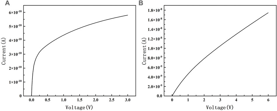
FIGURE 10. Leakage current curves v. s Bias voltage (A) Leakage current of Practical Novel 3D-Spherical-Electrode Detectors (B) Leakage current of traditional 3D-Trench electrode Si detectors.
Figure 11 shows the comparison of the leakage current of the Practical Novel 3D-Spherical-Electrode Detectors under different radiation intensities, with the increase of irradiation intensity, the leakage current of the detector increases. Because the carrier lifetime decreases under strong irradiation environment, we can see by Eq. 18 that the shorter the carrier lifetime, the higher the leakage current of the detector. Strong irradiation affects the performance of the detector (Li, 2021).
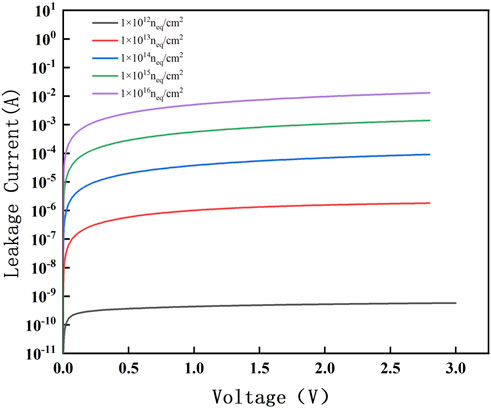
FIGURE 11. Leakage current of Practical Novel 3D-Spherical-Electrode Detectors with the influence of the radiation fluence.
Figure 12 shows the comparative capacitance curves of the two detectors, from which it can be seen that when the detector substrate is in a fully depleted state, its capacitance will not continue to change with the increase of the applied voltage. By comparison, the capacitance of the Practical Novel 3D-Spherical-Electrode Detectors is much smaller than that of the traditional 3D-Trench electrode Si detectors of the same size. One of the main factors affecting the noise is the capacitance of the detector, and the smaller the capacitance, the higher the signal-to-noise ratio and the better the performance of the detector.
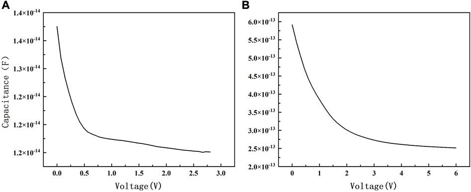
FIGURE 12. Capacitance curves v. s Bias voltage (A) Capacitance of Practical Novel 3D-Spherical-Electrode Detectors (B) Capacitance of traditional 3D-Trench electrode Si detectors.
Figure 13 shows the comparative capacitance of the Practical Novel 3D-Spherical-Electrode Detectors under different radiation intensities. Under radiation, when the bias voltage is low, the capacitance is large, and when the voltage reaches a certain value, the capacitance reaches the saturation capacitance. It can be seen that the radiation flux increases, the saturation capacitance remains the same and the capacitance size is only related to the structure of the detector itself (Tang, 2017).
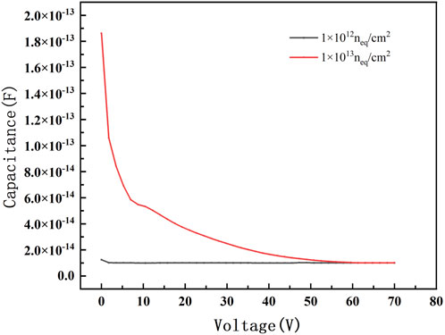
FIGURE 13. Capacitance of Practical Novel 3D-Spherical-Electrode Detectors With the influence of the radiation fluence.
The transient induced current and the weighting field of Practical Novel 3D-Spherical-Electrode Detectors
The induced current signal on detector electrodes was based on the Shockley–Ramo theorem (Liu et al., 2020b):
We set the LET_F (linear energy transfer) as 1.28 × 10⁻⁵, and set the wt_hi as 1 µm. Figure 14 shows the induced current curves we obtained by simulating the MIP (Minimum Ionising Particle) incidence from the middle position of the effective silicon body of the detector. The curve peaks are all located below 100 ps, and the response is extremely fast. The total charge is obtained by integrating the induced current. As the radiation flux increases, the total collected charge decreases and the response peaks become lower and lower, because increased irradiation causes defects that reduce the charge collection performance and the induced current, and radiation may also slightly affect the drift time (Liu et al., 2022).
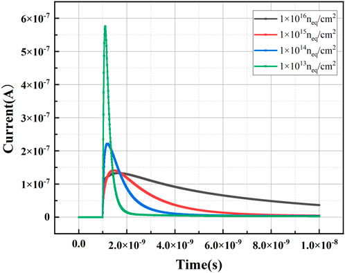
FIGURE 14. The induced current curves with time during radiation.
Figure 15A shows the 3D distribution of the weighting field of the detector array, and the 2D distribution is obtained by cross-sectioning the X-axis (Figure 15B), and the weighting field curve is obtained by intercepting the Z-axis (Figure 15C), which shows the weighting field in the immediate neighboring cell is practical zero, indicating that pressurizing one of the detectors that there will almost be no crosstalk between the two neighboring cells, and the coherence is weak. And as the Z-axis decreases, the specific weighting field becomes smaller, implying the outermost heavily doped ring of the detector plays a good isolation role.
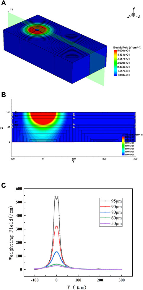
FIGURE 15. The (A) 3D (B) 2D; and (C) 1D weighting field distribution.
Conclusion
We have carried out extensive and systematic studies on our Practical Novel 3D-Spherical-Electrode Detectors using TCAD simulation software toll. The electrical characteristics such as electric potential, electric field, electron concentration, full depletion voltage, leakage current, capacitance, the induced transient current, weighting field were obtained. The detector performance after irradiation were also simulated and analyzed. All simulation results are compared with that of conventional 3D-Trench electrode Si detectors of the same size. The following conclusions are obtained:
1. The detector cathode electrode is of a spherical design with the same distance between anode and cathode everywhere in the detector, which makes the potential distribution in the detector symmetrical and uniform;
2. The design of the heavily doped ring on the upper surface makes the surface electric field distribution in the detector unit more uniform;
3. The full depletion voltage is small. The full depletion voltage is about -2.8 V for our example without irradiation, which is much lower than that of the traditional 3D-Trench electrode Si detectors of the same size.
4. The leakage current and capacitance of the detector are smaller, so the signal-to-noise ratio will be higher.
5. The detector response is fast and there is no crosstalk between array units.
6. The presence of a full-surface electrode on the bottom surface makes it easier to process in the detector fabrication.
Data availability statement
The original contributions presented in the study are included in the article/Supplementary Material, further inquiries can be directed to the corresponding author.
Author contributions
ZT and ZL contributed to conception and design of the study. XL and XC organized the database. ML and HW performed the statistical analysis. ZT wrote the first draft of the manuscript. All authors contributed to manuscript revision, read, and approved the submitted version.
Funding
This work was partly supported by the financial supports from Ludong University. The Key Scientific and Technological Innovation Project of Shandong Province (Grant No. 2019TSLH0316) and Yantai City-University Integration Development Project (No. 2020XDRHXMP11).
Conflict of interest
The authors declare that the research was conducted in the absence of any commercial or financial relationships that could be construed as a potential conflict of interest.
Publisher’s note
All claims expressed in this article are solely those of the authors and do not necessarily represent those of their affiliated organizations, or those of the publisher, the editors and the reviewers. Any product that may be evaluated in this article, or claim that may be made by its manufacturer, is not guaranteed or endorsed by the publisher.
Supplementary material
The Supplementary Material for this article can be found online at: https://www.frontiersin.org/articles/10.3389/fmats.2023.1149774/full#supplementary-material
References
Betta, G. F. D., Bagolini, A., Boscardin, M., Bosisio, L., and Zorzi, N. “Development of modified 3D detectors at FBK,” in Proceedings of the Nuclear Science Symposium Conference Record), Knoxville, TN, USA, October 2010.
Ding, H. (2015)., 796. Modeling and simulation of charge collection properties for 3D-trench electrode detector. Master. Xiangtan University.
Guo, J. F. a. Y. (2013). USA’s global infrared detecting equipment: Advancement, architecture analysis, and capability prediction. Infrared 34 (01), 1–9.
Li, X., Liu, M., and Li, Z. (2021). Design and simulation of silicon detector cells with spiral ring electrode structures. AIP Adv. 11 (4), 045127. doi:10.1063/5.0049765
Li, Z., Li, X., Cheng, W., and Li, Z. (2021). Radiation hardness property of ultra-fast 3D-Trench Electrode silicon detector on N-type substrate. Micromachines 12, 1400. doi:10.3390/mi12111400
Li, Z. (2011). New BNL 3D-Trench electrode Si detectors for radiation hard detectors for sLHC and for X-ray applications. Nucl. Inst. Methods Phys. Res. A 658 (1), 90–97. doi:10.1016/j.nima.2011.05.003
Liao, C. (2019). Research on the electrical properties and I-T curve of the adjustable center electrode type three-dimensional Trench Electrode silicon detector. Master, China: Xiangtan University.
Liu, M.-W., and Li, Z. “Development of ultra-fast 3D silicon detectors: 3D simulation and modeling of 3D-trench Electrode detector,” in Proceedings of the 3rd Annual International Conference on Advanced Material Engineering (AME 2017), January 2017.
Liu, M., Cheng, W., Li, Z., Zhao, Z., and Li, Z. (2022). 3D simulation, electrical characteristics and customized manufacturing method for a hemispherical electrode detector. Sensors 22 (18), 6835. doi:10.3390/s22186835
Liu, M., Li, Z., and Feng, M. (2017). 3D simulation and modeling of ultra-fast 3D silicon detectors. MATEC Web Conf. 108, 09006. doi:10.1051/matecconf/201710809006
Liu, M., Lu, S., and Li, Z. (2020a). Theoretical bases of hypothetical sphere-electrode detectors and practical near-sphere-electrode (semisphere-electrode and near-semisphere-electrode) detectors. J. Phys. D Appl. Phys. 54 (4), 045101. doi:10.1088/1361-6463/abbe48
Liu, M., Zhou, T., and Li, Z. (2020b). Electrical properties of ultra-fast 3D-Trench Electrode silicon detector. Micromachines 11 (7), 674. doi:10.3390/mi11070674
Liu, X. (2018). Study on electrical characteristics of low deadzone composite shell-electrode silicon detector. Master, China: Xiangtan University.
Lu, S. (2020). Study on electrical characteristics of novel hemispherical shell electrode silicon detector and array. Master, China: Xiangtan University.
Meng, X. (2009). “Development and application of new semiconductor detector technology,” in Proceedings of the Seventh Annual Conference of Chinese Society for Space Sciences). 188.
Meng, X. (2004). Development and application of new semiconducting detector. Nucl. Electron. Detect. Technol. (01), 87–96.
Ou, Y. (1998). Significance and prospect of nuclear energy utilization. WORLD SCI-TECH R&D (05), 28–31. doi:10.16507/j.issn.1006-6055.1998.05.010
Qin, W. (2007). Current status and development of medical imaging technology. Chin. J. Radiol. 41 (02), 113–114.
Tang, L. (2017). Simulation of electrical performance of open-close three-dimensional Trench Electrode silicon detector. Master, China: Xiangtan University.
Wei, W., and , J. Z. a. (2005). American early warning satellite probe and its related technology. Aerosp. China (06), 22–27+30.
Wu, C., Huang, X., Xiao, Y., and Li, Z. (2021). Design and simulation of a new silicon pixel detector with equal width floating electrodes. AIP Adv. 11 (2), 025315. doi:10.1063/5.0041850
Zhi-Ming, L. I., Wang, X., and Nie, J. S. (2017). Hole morphology in femtosecond laser drilling of silicon. Acta Photonica Sin.
Zhou, Y. (2013). Design and simulation of a 0.18 μm H-gate P-well SOI MOSFET device using sentaurus TCAD software. Electron. World (21), 95–96.
Keywords: 3D-Spherical Electrode Detectors, electric field distribution, electric potential distribution, fully depleted voltage, properties under radiation
Citation: Tan Z, Li Z, Li X, Cai X, Liu M and Wang H (2023) Study of electrical properties and detection mechanism of a practical novel 3D-Spherical Electrode Detector. Front. Mater. 10:1149774. doi: 10.3389/fmats.2023.1149774
Received: 23 January 2023; Accepted: 28 February 2023;
Published: 09 March 2023.
Edited by:
Ke Cao, Xidian University, ChinaReviewed by:
Libo Gao, Xiamen University, ChinaZinetula Z. Insepov, Purdue University, United States
Jiajia Liao, Xidian University, China
Copyright © 2023 Tan, Li, Li, Cai, Liu and Wang. This is an open-access article distributed under the terms of the Creative Commons Attribution License (CC BY). The use, distribution or reproduction in other forums is permitted, provided the original author(s) and the copyright owner(s) are credited and that the original publication in this journal is cited, in accordance with accepted academic practice. No use, distribution or reproduction is permitted which does not comply with these terms.
*Correspondence: Zheng Li, MzYzNkBsZHUuZWR1LmNu