 Yingfei Sun
 Yu Fang
 Zhongguo Li3
 Junyi Yang
 Yinglin Song
- 1School of Physical Science and Technology, Soochow University, Suzhou, China
- 2Jiangsu Key Laboratory of Micro and Nano Heat Fluid Flow Technology and Energy Application, School of Physical Science and Technology, Suzhou University of Science and Technology, Suzhou, China
- 3School of Electronic and Information Engineering, Changshu Institute of Technology, Changshu, China
- 4Department of Physics, Harbin Institute of Technology, Harbin, China
We report the different nonlinear optical mechanisms and defect-related carrier dynamics in Sn-doped β-Ga2O3 crystal by utilizing time-resolved pump-probe technique based on phase object under UV excitation. The obtained nonlinear optical parameters arise from bound electron can be well explained by the theoretical calculation of two-band model and Kramers-Kronig transformation. By tuning the probe wavelength, the carrier nonlinearity can be modulated greatly due to additional absorption of defects within the bandgap. The results reveal that by choosing a proper probe wavelength that matches the defect state to the valence band, the nonlinear absorption and refraction of the carriers can be greatly enhanced, which provides an important reference for the design of gallium oxide-based waveguide materials and all-optical switching materials in the future.
Introduction
Beta-phase gallium oxide (β-Ga2O3) is a transparent conductive oxide with an ultra-wide band gap of 4.9 eV (Tippins, 1965). It is also regarded as a promising candidate for UV detectors (Ji et al., 2006; Kokubun et al., 2007) and high-temperature gas sensors (Fleischer and Meixner, 1991; Liu et al., 2008). From the perspective of optoelectronic devices, it is very necessary to understand the optical properties of this material. Recently, many studies have been carried out to explore the electrical and optical properties of β-Ga2O3 (Suzuki et al., 2007; Mi et al., 2014; Chikoidze et al., 2016; Bhandari et al., 2019). However, reports on the nonlinear characteristics of β-Ga2O3 crystals under strong light are elusive.
In 2018, Hong Chen et al. used Z-Scan to measure the two-photon absorption coefficient and Kerr refractive index of gallium oxide (Chen et al., 2018), their research focuses on ultrafast nonlinear processes caused by bound electrons, but ignores the slow nonlinear processes associated with carriers. Okan Koksal et al. presented optical pump-probe spectroscopy results on defect-assisted recombination of photoexcited carriers in β-Ga2O3 (Koksal et al., 2018). They used a single wavelength to probe the additional carrier absorption of polarization-related defect states, but ignored the carrier refraction. The study of gallium oxide nonlinear absorption/refraction dynamics is of great significance to the design of all-optical switches and ultrafast optoelectronic devices. In 2020, Okan Koksal et al. verified the intra- and inter-conduction band optical absorption processes of β-Ga2O3 through steady state and ultrafast optical spectroscopy measurements (Singh et al., 2020), but they ignored the influence of defect state at 500-650 nm on absorption, which we will be explained explicitly in this paper. Gallium oxide has many impurities or intrinsic defects, such as Si, Sn, oxygen vacancy and gallium vacancy, which promote the radiative and nonradiative recombination of carriers (Varley et al., 2010; Dong et al., 2017; Neal et al., 2018). They can affect the photoelectric properties of materials, including conductivity, absorption, and even nonlinear optical properties (Yuksek et al., 2009; Ganesh et al., 2017; Bhandari and Zvanut, 2020; McCluskey, 2020). The reason why we choose Sn-doped β-Ga2O3 is that impurity Sn4+ instead of Ga3+ will generate additional free electrons (Zhang et al., 2010), so modulating the conduction band electron density by Sn doping is more conducive to measuring free carrier absorption.
In this paper, we studied the variation process of the nonlinear absorption/refraction of Sn-doped β-Ga2O3 with delay time by phase object pump-probe technique (POPP) at different probe wavelengths. The existence of the defect states is also proved by pump-probe spectroscopy. The bound electron-related and carriers-related nonlinear parameters as well as the defect state-related carrier dynamic processes are evaluated reasonably.
Experimental Section
The Sn-doped β-Ga2O3 (β-Ga2O3: Sn) crystal used in the experiment was a commercial single crystal material with the size of 5 × 10 × 0.68 mm3. The double-sided polished crystal had a monoclinic structure with a crystal orientation (
Q-switched and mode-locked Nd: YAG laser (355 nm, 8 ps) was employed as the degenerate POPP light sources. The laser is divided into two parts through the beam splitter: one part of the stronger energy is used as the pump light, and the other part of the weaker light after passing through the neutral density attenuator is used as the probe light. The light source of non-degenerate POPP is Yb: KGW femtosecond laser (Light Conversion, PHAROS-SP, 1,030 nm, 190 fs). The output laser beam is divided into two parts: a part of the higher energy light is used as the pump light, and the wavelength is tuned to 355 nm after passing through the optical parametric amplifier. The other part of the light with weaker energy is used as the probe light, and the wavelength becomes 515 nm after passing through the frequency doubling crystal. The schematic diagram of POPP is similar to our previous work (Sun et al., 2021). The pump light and probe light focus on the same point of the sample at a small angle (less than 5°), and the nonlinear dynamic process is explored by adjusting the delay time of the two beams. The probe light is focused on the sample after passing through the PO, and is directly received by the detector (open-aperture) after passing through the sample to obtain the nonlinear absorption response. If the aperture is closed (closed-aperture), the nonlinear refraction response of the sample can be obtained. The function of PO is to enhance the interference effect between the dielectric region and the outside region. The far-field diffraction pattern is greatly modulated after transmitting from the rear surface of the sample, so that the nonlinear phase shift signal of the sample is converted into the intensity signal. The experimental details were described explicitly in Yang et al. (2009a), Fang et al. (2013). The repetition rate was set to 10 Hz to avoid heat accumulation in the sample (Yang et al., 2009a; Yang et al., 2009b). The polarization of pump and probe beams were adjusted to be perpendicular in order to minimize the interference, where the pump beams were parallel to the (010) direction and the probe beams were parallel to the (102) direction. All measurements were performed at room temperature.
Results and Discussion
The nonlinear effects caused by bound electrons (two-photon absorption, Kerr refraction) are instantaneous, while the recovery time of the nonlinear effects caused by carriers (carrier absorption and carrier refraction) is relatively long. We can distinguish different nonlinear effects of samples by time-resolved POPP, and study the dynamics of nonlinear absorption/refraction of β-Ga2O3: Sn. The pump light with wavelength of 355 nm (3.49 eV) we choose satisfies the condition of Eg/2< ħωe < Eg, therefore two-photon absorption (TPA) of the pump beam may occur.
Degenerate POPP Experiment (355 nm for Pump and 355 nm for Probe)
β-Ga2O3: Sn was pumped and probed by 355 nm, excited under a peak intensity at 11 GW/cm2. Figure 1 shows the open-aperture 1) and closed-aperture 2) measurements of degenerate POPP for β-Ga2O3: Sn. It can be seen from 1) that there is a fast absorption process at the zero-delay position, which represents the degenerate TPA, and the weak tail behind represents the weak carrier absorption. At the same time, we get the closed-aperture curve as shown in 2). there is a negative weak Kerr refraction near zero delay, the tail behind represents the carrier induced refraction, and there is almost no recovery process of the tail with the delay time, which indicates that the carrier lifetime is long.
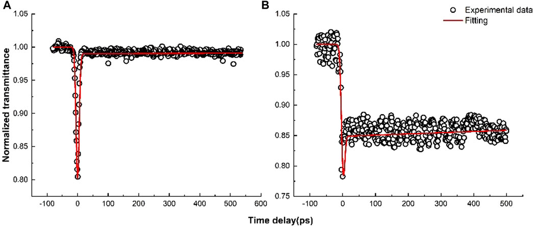
FIGURE 1. Nonlinear absorption curves (A) and nonlinear refraction curves (B) of β-Ga2O3: Sn at 355 nm pump and 355 nm probe.
Non-Degenerate POPP Experiment (355 nm for Pump and 515 nm for Probe)
As gallium oxide is a semiconductor with abundant energy bands, a large number of literatures have determined that the defect energy level of gallium oxide is between 2 and 3 eV above the valence band by means of luminescence spectroscopy and theoretical calculations. (Hajnal et al., 1999; Nakano, 2017; Gao et al., 2018). So we choose 515 nm (2.4 eV) to probe and observe the nonlinear absorption/refraction dynamics of β-Ga2O3: Sn. The peak intensity of pump light was set to 24 GW/cm2 and a faster femtosecond laser was used to study its ultrafast process.
Figure 2 shows the open-aperture 1) and closed-aperture 2) measurements of non-degenerate POPP for β-Ga2O3: Sn. It can be seen from 1) that the peak near the zero delay is caused by the non-degenerate TPA, and the tail behind is obviously deeper than that of the degenerate POPP. We speculate that the additional absorption causes the enhancement of carrier absorption. It is reported that Sn doping is a shallow donor level (Varley et al., 2010; Zhang et al., 2010), we did the same experiment on unintentionally doped (UID) gallium oxide, and found that there were similar results, proving that the additional absorption was not caused by doping, but may be caused by intrinsic defect in the growth process, as we will prove later. It can be seen from 2) that there is a weak peak caused by Kerr refraction near zero delay, which is different from the result of degenerate POPP. The tail behind represents carrier refraction. Since the non-degenerate POPP uses ultrafast laser, the recombination time is much longer than the detection window, and the recombination time is not significantly attenuated in the limited detection window, so we judge that the recombination time of the non-degenerate POPP is also very long at 515 nm (longer than 5 ns).
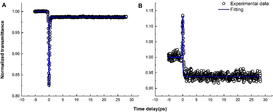
FIGURE 2. Nonlinear absorption curves (A) and nonlinear refraction curves (B) of β-Ga2O3: Sn at 355 nm pump and 515 nm probe.
Bound Electrons-Related Nonlinear Optical Parameters
When the incident laser pulse is Gaussian light, the light intensity distribution of the pump light on the front surface of the sample to be measured can be described by the following formula:
Where I0e is the peak light intensity of the pump light, ωe(z) = ω0e [1+(z/z0e)2]1/2 is the spot radius of the pump light at the sample to be measured, z is the distance between the sample to be measured and the beam waist of the pump light, z0e = πω0e2/λ is the Rayleigh (diffraction) length of the pump light, ω0e is the beam waist radius of the pump light, τd is the time delay between the pump light and the detection light.
According to the standard two-band model, in the case of weak probe light, it can be considered that the carrier generation mainly comes from the TPA of the pump light. So the equation rate of carriers can be expressed as (Sun et al., 2021):
In the formula, β is the TPA coefficient, Ie is the light intensity at the pump light sample, τr denote the recombination time (The overall time of direct recombination from conduction band to valence band and indirect recombination caused by defect states). The propagation formula of the probe light and pump light inside the β-Ga2O3: Sn crystal is (Sun et al., 2021):
In the formula, Ip and φp respectively represent the intensity and phase of the probe light, σ is absorption cross-section, n2 is the Kerr refractive index of the bound electron, and η is carrier refractive volume. According to the above rate Eqs 2–5, we fit bound electrons-related nonlinear optical parameters of degenerate and non-degenerate POPP, the results are listed in Table 1. In the following discussion, ωe denotes 355 nm pump beam and ωp1, ωp2 denote 355, and 515 nm probe beams respectively. We found that after changing the probe wavelength, the Kerr refraction changes from negative to positive.

TABLE 1. Bound electrons-related nonlinear optical parameters. β, TPA coefficient; n2, Kerr refractive index.
We further verify the accuracy of our TPA coefficient and Kerr refraction coefficient through the theoretical expression of the two-band model (Sheik-Bahae et al., 1991). The degenerate and nondegenerate TPA spectra predicted using:
Where Ep is related to the interband momentum matrix element and for the two-parabolic-band model is defined Ep = 2|Pvc|2/mo (Ep is approximately 21 eV for most semiconductors) (Kane, 1980), np and ne are the linear probe and pump refractive indices, respectively, F2 is the dimensionless spectral function, in Eq. 6, F2(x) =(2x−1)1.5/(2x)5, in Eq. 7, F2(x) =(x1+x2−1)1.5 (1/x1+1/x2)2/27 × 1 × 22 (Sheik-Bahae et al., 1991), K is ∼3,100 cm GW−1 eV5/2 (Hutchings and Van Stryland, 1992). According to this relationship, the calculated ratio of degenerate and non-degenerate TPA is 1.4, which is almost consistent with our experimental results. At the same time, we also measured 355 nm PS open-aperture Z-scan (as shown in Figure 3), and the fitted two-photon absorption coefficient (β = 1.1 × 10⁻¹¹ m/W) is three times larger than the degenerate POPP result, because the pump light and probe light in POPP are vertically polarized, resulting in the decrease of polarization tensor.
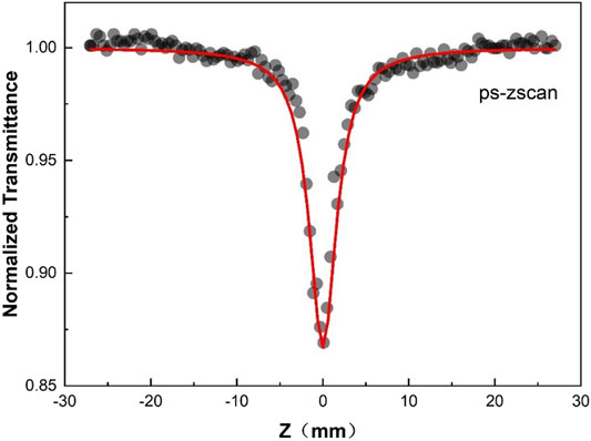
FIGURE 3. 355 nm PS open-aperture Z-scan for Ga2O3: Sn bulk crystals. The solid lines are the numerical fits to the experimental data.
The degenerate and non-degenerate n2 (ωp; ωe) is calculated via the Kramers-Kronig transformation resulting in (Sheik-Bahae et al., 1994; Zhao et al., 2016):
G2 is the dimensionless dispersion function (Sheik-Bahae et al., 1994). The calculated trend of the degenerate nonlinear refractive index n2 with ħω, from 0 to Eg/2, n2 increases to the maximum, and finally becomes negative as ħω approaches the band gap Eg. So the 355 nm (ħω/Eg = 0.71) Kerr refraction obtained by degenerate POPP tends to zero. The non-degenerate n2 (ωp; ωe) of β-Ga2O3: Sn crystal is calculated as a function of probe photon energy ħωp. n2 (ωp; ωe) is positive at low ωp. Due to the intermediate-state resonance enhancement, it increases to the maximum when ħωp = Eg–ħωe = 0.29 Eg. Then n2 (ωp; ωe) becomes abnormally dispersive and finally becomes negative when ωp approaches the band gap. Therefore, the results obtained from the non-degenerate (ħωe/Eg = 0.71, ħωp/Eg = 0.49) POPP meet the trend calculated by the two-band model, which is a positive value. We found that the theory is applicable to gallium oxide, and the refraction sign changed at different probe wavelengths.
Free Carrier -Related Nonlinear Optical Parameters
According to the above rate Eqs 2–5, we also fit free carrier-related nonlinear optical parameters of degenerate and non-degenerate POPP, the results are listed in Table 2. We found that after changing the probe wavelength, the responses of carrier absorption and refraction both increase by at least an order of magnitude. The increase of σ and η indicates that there indeed exists an additional absorption of defect state. We will explain in detail later.

TABLE 2. Free carrier -related nonlinear optical parameters. σ, FCA cross-section; η, FCR volume; τr, carrier lifetime.
In order to further verify the existence of the defect state, we focus the probe light on the sapphire to generate a white supercontinuum, thereby measuring the 500–650 nm transient absorption spectrum of β-Ga2O3: Sn crystal under two-photon excitation. The details of the experiment were described explicitly in Fang et al. (2016). The absorption results are shown in Figure 4. We can see that the transient absorption spectrum with different delay time shows broadband absorption, corresponding to a peak value of 550 nm (2.48 eV), and the profile and peak value of transient absorption have almost no change in the delay time of 6–1,100 ps. This is a typical defect state absorption. In Singh et al. (2020), they did the absorption spectra of different probe wavelengths (515, 600, 660, 800, 940 nm) under 450 nm excitation, and found that they were related to the transition in the conduction band (intraband free-carrier absorption) through α∝ω−3 fitting (Drude model, as shown by the red dotted line in Figure 4), while the extra absorption due to defect state between 500 and 650 nm is ignored. The difference between our experimental results and the Drude line proves the existence of defect state absorption.
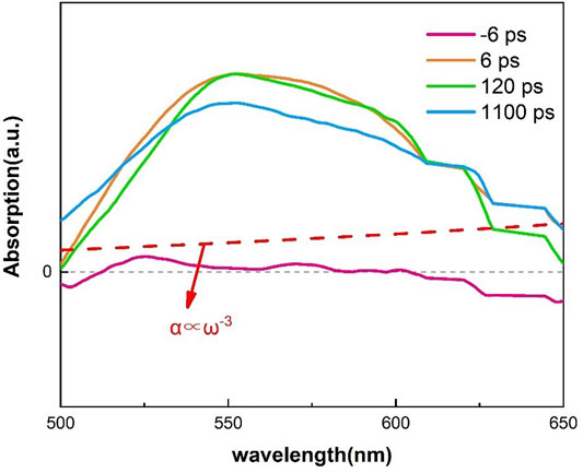
FIGURE 4. Transient absorption spectra of β-Ga2O3: Sn in 500–650 nm.
Next, we discuss the carrier dynamics of β-Ga2O3: Sn. It is reported that the effective mass of hole is much larger than that of electron (Yeo et al., 1998). According to Drude model, it can be considered that free carrier absorption and refraction mainly come from electrons. Since gallium oxide can be considered as a direct band gap semiconductor with a large band gap and low excited carrier concentration, the probability of direct recombination (radiation transition) is very low. Almost all carriers are recombined indirectly through defect energy levels (either radiation recombination or non-radiation recombination). As mentioned earlier, what we have probed is basically the response of electrons, so the dynamic process is dominated by the indirect recombination process of electrons.
In the case of degenerate POPP (355 nm pump, 355 nm probe), the valence band electrons can transition to the conduction band through degenerate TPA. When the probe light is incident on the semiconductor, electrons in the conduction band can continue to absorb a probe photon and transition to a higher conduction band energy level, which is free carrier absorption. Subsequently, the electrons transition to the defect state through indirect recombination, which leads to a decrease in the conduction band electron concentration, so that the absorption of free carriers under 355 nm detection is reduced, thereby forming a long tail (as shown in Figure 1).
In the case of non-degenerate POPP (355 nm pump, 515 nm probe), the valence band electrons are also excited by degenerate TPA and absorb the probe photons in the conduction band to produce carrier absorption (Corresponding to process A in Figure 5). At the same time, the pump light also excites the electrons in the defect state to the conduction band, which makes the defect state partially empty and makes it possible for the valence band electrons to transition to the defect state. Moreover, the probe photon energy just meets the energy level of the defect state (∼2.2 eV) extracted from transient absorption spectrum (Figure 4), so under non-degenerate conditions, the additional absorption of the defect state can be probed (Corresponding to process B in Figure 5). The increased σ and η obtained by non-degenerate POPP can be considered as a combination of free carrier effect (carrier dispersion effect) and defect state (absorption and refraction) effects, which cause the change in the real part and the imaginary part of the dielectric constant. Then the electron transitions to the defect state through indirect recombination (Corresponding to τr in Figure 5). This also leads to a decrease in the conduction band electron concentration, so that the free carrier absorption under 515 nm probe is reduced, and secondly, due to the indirect recombination of the electron transition to the defect state, causing the defect state to be partially occupied, so that the defect state’s absorption of the 515 nm probe is reduced. Therefore, based on the previous experimental results, it can be judged that the indirect recombination time under non-degenerate POPP is also in the order of nanoseconds.
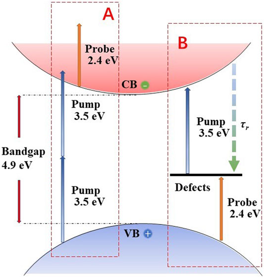
FIGURE 5. Schematic diagram of the energy levels and carrier decay processes of β-Ga2O3: Sn. The blue up arrow represents the two-photon excitation, the green down arrow represents the recombination process related to the defect state, and the orange up arrow represents the transition from the valence band to the defect state.
In Table 3, we list the nonlinear optical parameters of more popular semiconductor materials recently. Through comparison, we not only find that our test methods can accurately obtain more comprehensive nonlinear optical parameters, but also find that the nonlinear absorption and refraction are relatively small compared with other materials, which means that as a waveguide material, it has lower loss (Lin et al., 2007; Sierra et al., 2019), and β-Ga2O3 can be used as a substrate under the growth conditions of GaN-based compounds (Ohira et al., 2008), which shows that gallium oxide is expected to be used in integrated photonics applications. The transformation of refraction symbol and carrier lifetime also show the potential application value of gallium oxide in the field of ultrafast all-optical switching (Nozaki et al., 2010; Fang et al., 2015). Therefore, it is very important to understand these parameters, which provides an important reference for the design of gallium oxide optoelectronic devices in the future.

TABLE 3. Photo-physical parameters of β-Ga2O3: Sn, GaN, ZnO and UID β-Ga2O3. Eg, bandgap; Ee/Eg, relative photon energy; β, TPA coefficient; σ, FCA cross-section; n2, kerr refractive index; η, FCR volume; τr, carrier lifetime.
Conclusion
In summary, POPP technologies were utilized to discuss the optical nonlinear response of Sn-doped β-Ga2O3 crystal under excitation at 355 nm and the defect state dependent carrier dynamics. The corresponding parameters at different probe wavelengths were obtained through rate equation model fitting. We find that the sign of Kerr refraction changed from negative to positive, which satisfies the theoretical calculation of the two-band model under the Kramers-Kronig relationship. Moreover, when the probe photon energy satisfies the defect state transition to the valence band, the carrier absorption cross-section and the carrier refraction volume are increased by at least an order of magnitude, which indicates that the carrier absorption and refraction caused by defect states are wavelength-dependent parameters. Understanding the carrier dynamics and nonlinear optical parameters is essential for the development of β-Ga2O3 technology, and provides important references for future design based on all-optical switches and optical waveguide devices.
Data Availability Statement
The original contributions presented in the study are included in the article/Supplementary Material, further inquiries can be directed to the corresponding authors.
Author Contributions
YFS, YF, ZL, and YLS contributed to conception and design of the study. JY, XW, and JJ contributed to experiments and data fitting. KL and LC contributed to manuscript revision. All authors contributed to read, and approved the submitted version.
Conflict of Interest
The authors declare that the research was conducted in the absence of any commercial or financial relationships that could be construed as a potential conflict of interest.
The handling Editor declared a past co-authorship with one of the author YS.
Publisher’s Note
All claims expressed in this article are solely those of the authors and do not necessarily represent those of their affiliated organizations, or those of the publisher, the editors and the reviewers. Any product that may be evaluated in this article, or claim that may be made by its manufacturer, is not guaranteed or endorsed by the publisher.
Acknowledgments
We gratefully acknowledge the NSAF (Grant No. U1630103), Special Fund from State Key Laboratory of Intense Pulsed Radiation Simulation and Effect (No. SKLIPR1715), National Natural Science Foundation of China (No. 11704273, 11804244), Natural Science Foundation of Jiangsu Province, China (Grant No. BK20180965).
References
Bhandari, S., and Zvanut, M. E. (2020). Optical Transitions for Impurities in Ga2O3 as Determined by Photo-Induced Electron Paramagnetic Resonance Spectroscopy. J. Appl. Phys. 127, 065704. doi:10.1063/1.5140193
Bhandari, S., Zvanut, M. E., and Varley, J. B. (2019). Optical Absorption of Fe in Doped Ga2O3. J. Appl. Phys. 126, 165703. doi:10.1063/1.5124825
Chen, H., Fu, H., Huang, X., Montes, J. A., Yang, T.-H., Baranowski, I., et al. (2018). Characterizations of the Nonlinear Optical Properties for (010) and (2 01) Beta-phase Gallium Oxide. Opt. Express 26, 3938–3946. doi:10.1364/oe.26.003938
Chikoidze, E., Von Bardeleben, H. J., Akaiwa, K., Shigematsu, E., Kaneko, K., Fujita, S., et al. (2016). Electrical, Optical, and Magnetic Properties of Sn Doped α-Ga2O3 Thin Films. J. Appl. Phys. 120, 025109. doi:10.1063/1.4958860
Dong, L., Jia, R., Xin, B., Peng, B., and Zhang, Y. (2017). Effects of Oxygen Vacancies on the Structural and Optical Properties of β-Ga2O3. Sci. Rep. 7, 40160. doi:10.1038/srep40160
Fang, Y., Yang, J. Y., Yang, Y., Wu, X., Xiao, Z., Zhou, F., et al. (2016). Ultrafast Carrier Dynamics in a P-type GaN Wafer under Different Carrier Distributions. J. Phys. D Applied Phys. 49, 045105. doi:10.1088/0022-3727/49/4/045105
Fang, Y., Wu, X.-Z., Ye, F., Chu, X.-Y., Li, Z.-G., Yang, J.-Y., et al. (2013). Dynamics of Optical Nonlinearities in GaN. J. Appl. Phys. 114, 103507. doi:10.1063/1.4820929
Fang, Y., Xiao, Z., Wu, X., Zhou, F., Yang, J., Yang, Y., et al. (2015). Optical Nonlinearities and Ultrafast All-Optical Switching of M-Plane GaN in the Near-Infrared. Appl. Phys. Lett. 106, 251903. doi:10.1063/1.4923184
Fleischer, M., and Meixner, H. (1991). Gallium Oxide Thin Films: A New Material for High-Temperature Oxygen Sensors. Sensors Actuators B: Chem. 4, 437–441. doi:10.1016/0925-4005(91)80148-d
Ganesh, V., Yahia, I. S., Alfaify, S., and Shkir, M. (2017). Sn-doped ZnO Nanocrystalline Thin Films with Enhanced Linear and Nonlinear Optical Properties for Optoelectronic Applications. J. Phys. Chem. Sol. 100, 115–125. doi:10.1016/j.jpcs.2016.09.022
Gao, H., Muralidharan, S., Pronin, N., Karim, M. R., White, S. M., Asel, T., et al. (2018). Optical Signatures of Deep Level Defects in Ga2O3. Appl. Phys. Lett. 112, 242102. doi:10.1063/1.5026770
Hajnal, Z., Miró, J., Kiss, G., Réti, F., Deák, P., Herndon, R. C., et al. (1999). Role of Oxygen Vacancy Defect States in Then-type Conduction of β-Ga2O3. J. Appl. Phys. 86, 3792–3796. doi:10.1063/1.371289
Hutchings, D. C., and Van Stryland, E. W. (1992). Nondegenerate Two-Photon Absorption in Zinc Blende Semiconductors. J. Opt. Soc. Am. B 9, 2065. doi:10.1364/josab.9.002065
Ji, Z., Du, J., Fan, J., and Wang, W. (2006). Gallium Oxide Films for Filter and Solar-Blind UV Detector. Opt. Mater. 28, 415–417. doi:10.1016/j.optmat.2005.03.006
Kane, E. (1980). “Band Structure of Narrow gap Semiconductors,” in Narrow Gap Semiconductors Physics and Applications (Berlin: Springer), 13–31.
Koksal, O., Tanen, N., Jena, D., Xing, H., and Rana, F. (2018). Measurement of Ultrafast Dynamics of Photoexcited Carriers inβ-Ga2O3by Two-Color Optical Pump-Probe Spectroscopy. Appl. Phys. Lett. 113, 252102. doi:10.1063/1.5058164
Kokubun, Y., Miura, K., Endo, F., and Nakagomi, S. (2007). Sol-gel Prepared β-Ga2O3 Thin Films for Ultraviolet Photodetectors. Appl. Phys. Lett. 90, 031912. doi:10.1063/1.2432946
Li, Z.-g., Yang, J.-y., Wei, T.-H., and Song, Y.-l. (2013). Intensive Two-Photon Absorption Induced Decay Pathway in a ZnO crystal: Impact of Light-Induced Defect State. Appl. Phys. Lett. 103, 252107. doi:10.1063/1.4855375
Lin, Q., Painter, O. J., and Agrawal, G. P. (2007). Nonlinear Optical Phenomena in Silicon Waveguides: Modeling and Applications. Opt. Express 15, 16604–16644. doi:10.1364/oe.15.016604
Liu, Z., Yamazaki, T., Shen, Y., Kikuta, T., Nakatani, N., and Li, Y. (2008). O2 and CO Sensing of Ga2O3 Multiple Nanowire Gas Sensors. Sensors Actuators B: Chem. 129, 666–670. doi:10.1016/j.snb.2007.09.055
Mi, W., Du, X., Luan, C., Xiao, H., and Ma, J. (2014). Electrical and Optical Characterizations of β-Ga2O3:Sn Films Deposited on MgO (110) Substrate by MOCVD. RSC Adv. 4, 30579. doi:10.1039/c4ra02479f
Nakano, Y. (2017). Communication-Electrical Characterization of β-Ga2O3 Single Crystal Substrates. ECS J. Solid State. Sci. Technol. 6, P615–P617. doi:10.1149/2.0181709jss
Neal, A. T., Mou, S., Rafique, S., Zhao, H., Ahmadi, E., Speck, J. S., et al. (2018). Donors and Deep Acceptors in β-Ga2O3. Appl. Phys. Lett. 113, 062101. doi:10.1063/1.5034474
Nozaki, K., Tanabe, T., Shinya, A., Matsuo, S., Sato, T., Taniyama, H., et al. (2010). Sub-femtojoule All-Optical Switching Using a Photonic-crystal Nanocavity. Nat. Photon. 4, 477–483. doi:10.1038/nphoton.2010.89
Ohira, S., Suzuki, N., Arai, N., Tanaka, M., Sugawara, T., Nakajima, K., et al. (2008). Characterization of Transparent and Conducting Sn-Doped β-Ga2O3 Single crystal after Annealing. Thin Solid Films 516, 5763–5767. doi:10.1016/j.tsf.2007.10.083
Sheik-Bahae, M., Hutchings, D. C., Hagan, D. J., and Van Stryland, E. W. (1991). Dispersion of Bound Electron Nonlinear Refraction in Solids. IEEE J. Quan. Electron. 27, 1296–1309. doi:10.1109/3.89946
Sheik-Bahae, M., Wang, J., and van Stryland, E. W. (1994). Nondegenerate Optical Kerr Effect in Semiconductors. IEEE J. Quan. Electron. 30, 249–255. doi:10.1109/3.283767
Sierra, J. H., Rangel, R. C., Samad, R. E., Vieira, N. D., Alayo, M. I., and Carvalho, D. O. (2019). Low-loss Pedestal Ta2O5 Nonlinear Optical Waveguides. Opt. Express 27, 37516–37521. doi:10.1364/oe.27.037516
Singh, A., Koksal, O., Tanen, N., McCandless, J., Jena, D., Xing, H., et al. (2020). Intra- and Inter-conduction Band Optical Absorption Processes in β-Ga2O3. Appl. Phys. Lett. 117, 072103. doi:10.1063/5.0016341
Sun, Y., Fang, Y., Li, Z., Yang, J., Zhou, W., Liu, K., et al. (2021). Free Carrier-Induced Optical Nonlinearities in β-Ga2O3 Single Crystals at 355 Nm. J. Phys. D: Appl. Phys. 54, 495105. doi:10.1088/1361-6463/ac24c6
Suzuki, N., Ohira, S., Tanaka, M., Sugawara, T., Nakajima, K., and Shishido, T. (2007). Fabrication and Characterization of Transparent Conductive Sn-Doped β-Ga2O3 Single crystal. Phys. Stat. Sol. 4, 2310–2313. doi:10.1002/pssc.200674884
Tippins, H. H. (1965). Optical Absorption and Photoconductivity in the Band Edge ofβ−Ga2O3. Phys. Rev. 140, A316–A319. doi:10.1103/physrev.140.a316
Varley, J. B., Weber, J. R., Janotti, A., and Van de Walle, C. G. (2010). Oxygen Vacancies and Donor Impurities in β-Ga2O3. Appl. Phys. Lett. 97, 142106. doi:10.1063/1.3499306
Yang, J., Song, Y., Wang, Y., Li, C., Jin, X., and Shui, M. (2009). Time-resolved Pump-Probe Technology with Phase Object for Measurements of Optical Nonlinearities. Opt. Express 17, 7110–7116. doi:10.1364/oe.17.007110
Yang, J., Zhang, X., Wang, Y., Shui, M., Li, C., Jin, X., et al. (2009). Method with a Phase Object for Measurement of Optical Nonlinearities. Opt. Lett. 34, 2513–2515. doi:10.1364/ol.34.002513
Yeo, Y. C., Chong, T. C., and Li, M. F. (1998). Electronic Band Structures and Effective-Mass Parameters of Wurtzite GaN and InN. J. Appl. Phys. 83, 1429–1436. doi:10.1063/1.366847
Yuksek, M., Elmali, A., Karabulut, M., and Mamedov, G. M. (2009). Switching from Negative to Positive Nonlinear Absorption in P Type 0.5 at% Sn Doped GaSe Semiconductor crystal. Opt. Mater. 31, 1663–1666. doi:10.1016/j.optmat.2009.04.003
Zhang, Y., Yan, J., Zhao, G., and Xie, W. (2010). First-principles Study on Electronic Structure and Optical Properties of Sn-Doped β-Ga2O3. Phys. B: Condens. Matter 405, 3899–3903. doi:10.1016/j.physb.2010.06.024
Keywords: Ga2O3, nonlinear optical, defect state, pump probe technique, carrier dynamic
Citation: Sun Y, Fang Y, Li Z, Yang J, Wu X, Jia J, Liu K, Chen L and Song Y (2021) Ultrafast Dynamics of Optical Nonlinearities in β-Ga2O3. Front. Mater. 8:754842. doi: 10.3389/fmats.2021.754842
Received: 07 August 2021; Accepted: 15 October 2021;
Published: 01 November 2021.
Edited by:
Zhongquan Nie, Taiyuan University of Technology, ChinaCopyright © 2021 Sun, Fang, Li, Yang, Wu, Jia, Liu, Chen and Song. This is an open-access article distributed under the terms of the Creative Commons Attribution License (CC BY). The use, distribution or reproduction in other forums is permitted, provided the original author(s) and the copyright owner(s) are credited and that the original publication in this journal is cited, in accordance with accepted academic practice. No use, distribution or reproduction is permitted which does not comply with these terms.
*Correspondence: Yu Fang, eXVmYW5nQHVzdHMuZWR1LmNu; Yinglin Song, eWxzb25nQGhpdC5lZHUuY24=