 Florian HörichChristopher Lüttich
 Jona GrümbelJürgen BläsingMartin Feneberg
 Armin Dadgar*Rüdiger Goldhahn
 André Strittmatter
- Otto-von-Guericke-Universität Magdeburg, Institut für Physik, Magdeburg, Germany
Implementing transition metal nitride (TM-nitride) layers by epitaxy into group-III nitride semiconductor layer structures may solve substantial persisting problems for electronic and optoelectronic device configurations and subsequently enable new device classes in the favorable nitride semiconductor family. As a prominent example, the integration of the group-III-transition metal nitride AlScN enabled an improved performance of GaN based transistor structures due to stronger polarization fields as has been recently demonstrated. For other transition metal nitrides (TMNs) and their alloys with group-III nitrides a range of other interesting properties is expected to enable novel devices and applications. We investigated the compatibility of TM-nitride layers with the growth of GaN-based structures on silicon substrates. As we show TiN layers are compatible and particularly suited as highly conducting, metallic-like buffer layer enabling true vertical conduction without elaborate backside processing. Also, we demonstrate epitaxial growth of alloys based on ScN and AlN as well as of HfN layers on Si(111) substrates by reactive sputtering using high purity gases and targets. Particularly, we analyzed the crystal structure and the quality of Sc-rich AlxSc1-xN. For HfN layers, we find a unique impact on the growth polarity of MOVPE-grown GaN layers on Si(111) which changes to N-polar growth. This represents a simple and technologically scalable approach for N-polar GaN-based layers on Si substrates.
Introduction
In the past decades group-III-nitrides have changed our daily live, as GaN based light emitting diodes (Nakamura et al., 1993) are nowadays the source of energy efficient light emission in general lighting but also in most display technologies. In addition, GaN electronics has become a serious competitor to Si but also to SiC in applications up to 1200 V as an energy efficient material (Abid et al., 2022). In particular, lateral high electron mobility transistors (HEMT) are often based on AlGaN/GaN heterostructures where an electron channel forms at the interface due to inherent polarization effects (Mohammad et al., 1995). AlInN/GaN heterostructures provide even higher channel conductivity (Dadgar et al., 2004) although devices thereof have not made it into market. Another material that recently came into focus is AlScN, which is ferroelectric in a wide composition range and can be integrated with GaN-based structures. For example, high power AlScN/GaN based HEMTs were demonstrated (Ligl et al., 2020; Krause et al., 2023). Still, this material has only been scarcely investigated as the epitaxial growth across the full compositional range is challenging. When grown by MOVPE, a columnar morphology and high surface roughness appear (Wolff et al., 2024; Streicher et al., 2024) in contrast to growth of AlGaN or AlInN layers, which yields contiguous, smooth films. It can be therefore expected that structural improvements over the whole composition range will lead to a better understanding of materials properties. To investigate these properties from the Sc-rich side we have prepared AlScN on ScN buffer layers. As ScN crystallizes in the rock-salt structure (Mihalic et al., 2023) one would expect a transition to the wurtzite crystal structure with increasing Al-content in AlScN. The transition itself as well as the resulting structural properties can be compared with the growth of AlScN with increasing Sc content on wurtzite AlN buffers.
Due to constraints set by heteroepitaxy of group-III nitrides on foreign substrates, most GaN-based devices are either lateral (HEMTs) or pseudo vertical devices (LEDs) (Nakamura et al., 1993; Mohammad et al., 1995). The use of expensive GaN substrates enables true vertical conduction (Kanechika et al., 2007; Chowdhury et al., 2013). GaN-on-Si technology allows for labor-intensive layer transfer technologies and backside-etching of Si substrates and Al-rich buffer layers (Hamdaoui et al., 2024a; Hamdaoui et al., 2024b). If a member of the TMN family could be applied as a metallic compliant interlayer, it could provide unprecedented electrical conductivity, which would allow to homogenize vertical current flow through epitaxial layer stacks grown on non-conductive buffer layers or substrates. Armitage et al. demonstrated in 2002 the usage of a HfN buffer for the growth of GaN (Armitage et al., 2002). HfN is a mechanically hard and thermally as well as chemically robust metal. TiN is also well known as hard surface coating on drilling tools but also known for metallic behavior. Therefore, TiN and HfN bear great potential as conducting buffer layer or interlayer in GaN layer structures. However, little is known about the preparation steps necessary for these TMN in order to facilitate their implementation into MOVPE processes for nitride devices. We first introduce general considerations regarding issues for the implementation of TMN in nitride epitaxy. A crucial point for epitaxy is the in-plane atomic distance of the rock-salt (111) and wurtzite (0001) planes. As seen in the map in Figure 1, best suited seems ScN which lies between GaN and AlN, but also ZrN, HfN, NbN and TaN show low a mismatch of <1–2%. Apart from these obviously low lattice mismatch compounds, the mismatch of TiN to AlN is not much larger than between AlN and GaN. As the metal nitrides all have larger thermal expansion coefficients compared to Si, in typical growth processes tension will build up in grown films which may lead to cracking (Dadgar et al., 2000) and wafer bow (Dadgar et al., 2013). Thus, layer stacks with increasing lattice parameter or atomic distance have to be considered to build up compression in the growing film. TiN is in principle interesting for overgrowth with high Al-content layers as a buffer layer provided that compressive growth of, e.g., AlN on top is successful. This motivates our choice of TiN among the TMN binaries. ScN, showing semiconducting behavior, and HfN, showing metallic behavior, are promising due to their particularly low lattice mismatch to AlN and GaN, respectively.
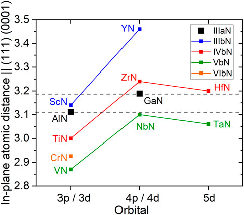
Figure 1. Map of potential transition metal nitrides and their in-plane atomic distance in comparison to AlN and GaN. ScN and HfN show lowest lattice mismatch to AlN and GaN while TiN and ZrN are also interesting for group-III-nitride growth on top. NbN as superconducting material is perfectly suited for low temperature applications but shows a high reactivity with oxygen. ScN is a semiconductor while TiN, HfN and ZrN show metallic properties.
Experimental
Growth of transition-metal-nitride layers was performed in a custom-built UHV sputtering system originally designed for group-III-nitride epitaxy with a heated and rotating 4 inch sample holder (up to 1000°C) and several 2 and 4 inch magnetrons being spherically placed at about 15 cm distance from the sample position. The base pressure of the system is 5 × 10⁻⁹ mbar. All targets were pure metallic targets with highest purity available ranging from 7N for Ga, via 6N for Al to 4N for Ti and 3N5 for Hf and Sc. As gases one can use getter purified Ar, H2, N2, and NH3. Sample growth was performed on (111) oriented p-Si substrates. Some of the HfN and TiN layers were overgrown by MOVPE in an AIX 200/4 RF-S system to investigate their compliance with group-III nitride epitaxy. In case of HfN, the MOVPE process comprised a first layer of ∼100 nm AlN followed by ∼400 nm GaN. MOVPE overgrowth of TiN started with an initial 2 nm thin AlN:Si layer followed by two thicker AlGaN:Si layers with increasing Ga-content and a final GaN layer doped with either Si or Ge to enable vertical electrical measurements. The usage of AlN is required to achieve a good seeding on the transition metal nitride buffer. Without this initial layer, no homogenous GaN layer could be grown yet. The AlGaN layers are helpful for strain engineering to avoid cracking of GaN (Dadgar et al., 2013). It has to be pointed out that all layers show c-plane orientation in growth direction but also low twist of grains around the surface normal which manifests in x-ray diffraction ω-full widths at half maximum (FWHM) comparable to or even better than for some of the best MOVPE-grown AlN layers on Si(111) (Dadgar et al., 2006).
ScN and AlScN
Commercially available precursors for MOVPE of ScN, namely, oxygen-free Sc-precursors, generally have a low vapor pressure. Thus, they require high precursor temperatures, heated gas lines and still yield low growth rates (<250 nm/h) of AlScN particularly for Sc-rich alloys (Streicher et al., 2024; Leone et al., 2019). As an alternative we developed a process by sputter epitaxy (SpE) that offers higher growth rates (typically 0.5–1 μm/h) thus enabling thicker layers and a high crystalline quality. For mapping the growth of AlScN over the full range, we consider the choice of AlN or ScN as buffer layer as important since the initial layer AlScN structure will be forced onto a rock-salt structure (for ScN) or a wurtzite structure (for AlN). A structural transition of the AlScN crystal lattice from rock-salt to wurtzite is expected in the range of [Al] = 40–60%. Here we present AlScN layers grown on ScN. Sputtering of ScN was optimized first to obtain a high crystalline quality, namely, low XRD ω-FWHMs for the out-of-plane and in-plane reflections, as well as a smooth surface quality. Growth temperatures of 800°C–900°C yield the best (111) XRD FWHM of around 2° for a layer thickness of 100 nm. Further optimization was achieved by introducing a metallic Sc layer on the Si surface with a nominal thickness of about two monolayers. This is similar to SpE as well as to MOVPE of AlN on Si where we also include a thin nucleation layer (Hörich et al., 2021). This reduced the XRD FWHM to about 1.3°. Further, the choice of the reactive gas (e.g., the nitrogen supply gas) is critical. Similar to our earlier observations for the case of AlN SpE (Dadgar et al., 2022) it is imperative to start sputtering of ScN on Si with nitrogen. After the growth of about 50 nm it is beneficial for obtaining smoother layer surfaces to use ammonia. Although evidence from a microscopic analysis has yet to be demonstrated, we assume that the high reactivity of ammonia with Si is leading to a fast nitridation at the early stage of growth. Surface nitridation of Si destroys the epitaxial relationship with the layer. Figure 2 shows the cross sectional scanning electron microscopy (SEM) image of a ScN layer followed by a nearly identically thick AlScN layer. As can be seen, ScN grown on Si shows a columnar structure (Figure 2A) which continues for the AlScN grown on top. For AlScN growth on ScN at various power levels applied to the Al-target we observe a power dependent shift of the Θ-2Θ AlScN(0002) diffraction peak (Figures 2B, C) which monitors the molar composition. At an Al-content of ∼45% the diffraction peak intensity significantly decreases indicating the beginning of unstable growth of AlScN on cubic ScN. This is also reflected by the AlScN(111) ω-FWHM (Figure 3) which starts at 1° for an Al-content close to 0% (20 W target power), reaches a minimum of 0.8° at an Al-content around 8% (50 W) and then slowly increases up to 1.2° for an Al-content of ∼41% (100 W). It then jumps to a much higher value of 1.85° at an Al-content of ∼45% (120 W) likely due to the beginning instability of the cubic and an increasing stability of the wurtzite phase. Here also the peak intensity decreases significantly and one can conclude that the highest Al-composition of stable cubic AlScN on ScN is between 41% and 45%.
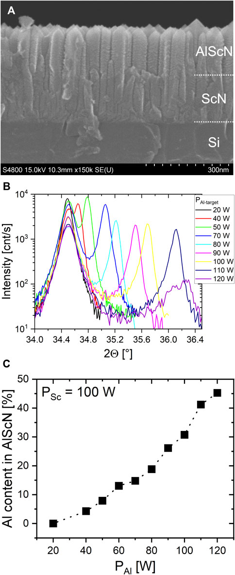
Figure 2. (A) SEM cross section image of AlScN on ScN with approximately identical layer thicknesses. (B) XRD Θ-2Θ scans of the samples and (C) determined AlScN concentration up to an Al content of 45% for AlScN grown on ScN(111). At 45% a degradation of the diffraction signal can be observed.
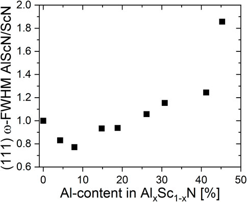
Figure 3. Dependence of the AlScN ω-FWHM on the Al-content in AlScN, see also Figure 2C.
HfN
The suitability of HfN as a buffer for molecular beam epitaxy of GaN on Si was already demonstrated by Armitage et al. (2002). They demonstrate crack free GaN on nearly lattice matched magnetron sputtered HfN on Si(111) and Si(001) with a crack-free thickness of 1 and 1.2 µm, respectively. The crystalline quality was reasonably good with an XRD FWHM of ∼1140“. The rms roughness was 10 nm and thus much inferior to state-of-the-art GaN. Unfortunately, no surface image was shown as we have strong indications that HfN can switch the polarity of GaN to N-polar. With the Hf-precursor tetrakis(dimethylamido)hafnium, having a reasonable vapor pressure when used at precursor temperatures above 60°C in MOVPE systems, one can in principle grow HfN by MOVPE. On Si there is the problem that Hf in this precursor is directly bound to four N-atoms thus standard growth schemes, similar to the initial phase of growth in SpE with a nominally metallic deposition on Si is likely difficult to achieve. In addition, because of the lack of heated precursor lines, we have grown HfN by SpE as this method is cheaper, offers higher growth rates and, in particular, very good crystallographic properties are achieved with this method. The growth of HfN by SpE is similar to the growth of other metal nitrides. A nominally two monolayer thin, metallic nucleation layer is deposited followed by the growth of HfN with a N2/Ar mixture. Growth temperatures of 900°C improve the crystalline quality to values of 0.68° for the (111) HfN ω-FWHM (Figure 4A). As reported before (Sproul, 1984), increasing the amount of nitrogen leads to a slight color change from light gold to golden. We also grew HfN with NH3 to compare the reactivity of the nitrogen precursor. As described in reference (Perry et al., 1988) we also observe a color change, now from golden to transparent films with interference fringes. This indicates the formation of an energy gap. A change of the lattice structure from rocksalt HfN to the nitrogen-rich orthorhombic semiconductor Hf3N4 (Salamat et al., 2013) could explain this observation.
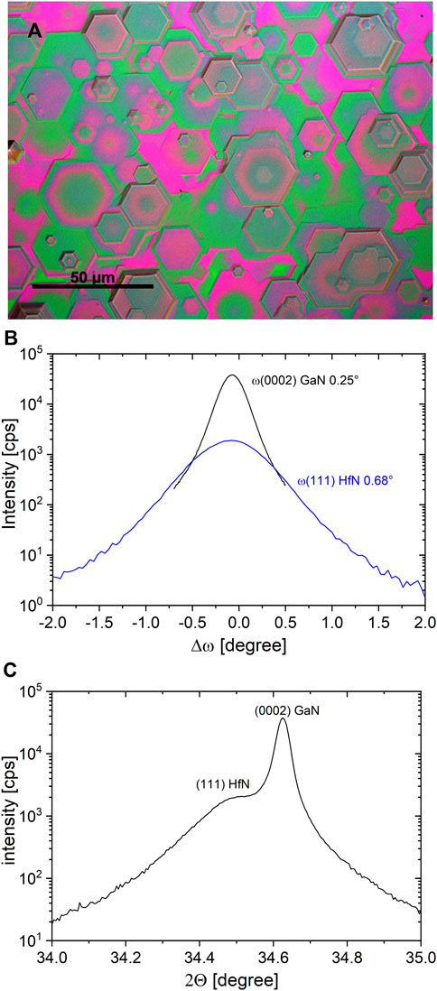
Figure 4. (A): Nomarski microscope image of ∼400 nm of GaN on AlN on SpE HfN. The surface structure is typical for N-polar GaN as confirmed by KOH etching (Weyher et al., 2003). (B): ω-scan of the GaN (0002) and HfN(111) reflections demonstrating the good crystalline quality. (C): Θ-2Θ scan of the sample.
Overgrowth of HfN with GaN was performed by MOVPE. The surface morphology observed (Figure 4B) is typical for nitrogen polar GaN as confirmed by KOH etching (Weyher et al., 2003). Although only 400 nm thick, large islands with flat surfaces and diameters up to ∼20 µm are visible. Being able to control the polarity of GaN on Si substrates in a simpler way as compared to excessive Mg-doping (Pezzagna et al., 2004) makes HfN a very interesting material for N-polar GaN based devices. For device structures an improvement of the surface morphology is required, however. By XRD measurements, in particular taking into account the low thickness of the MOVPE grown GaN layer, a good GaN quality is confirmed with FWHM values as low as 0.25° (900“) in ω-scans around the (0002) reflection (Figure 4A). Figure 4C displays corresponding Θ-2Θ scans where two diffraction peaks are observed along with a very small diffraction peak from AlN at larger angles (not shown).
TiN
As compared to ScN and HfN to GaN, TiN shows a relatively high lattice mismatch to AlN, but comparable to the one between AlN and GaN. In particular, its high chemical stability makes it suited to replace AlN in typical GaN device stacks, which include Al-rich strain engineering layers in the buffer. Such AlGaN layers, if the Al-content is chosen not too high, can be doped with Si or Ge, enabling good vertical conduction. The growth of TiN can be conducted by MOVPE or SpE. With TiCl4, a suited liquid high vapor pressure precursor for MOVPE of TiN is available. However, strong pre-reactions with ammonia can occur and, in our experiments, the quality of MOVPE TiN is still inferior to sputtered TiN. We measured FWHM values for ω-scans around the (111) reflection of 2.1° (MOVPE) and 0.13° (SpE) and around the (220) reflection of 1.5° (MOVPE) and 0.33° (SpE), respectively.
For SpE of TiN one has to pay attention to the high reactivity of Ti with many other elements. For instance, it makes Ti an often used getter material in UHV systems. Thus, an ultra-high vacuum chamber and high purity sources are required to avoid contaminations with, e.g., oxygen. As in the case of Sc and Hf a thin metallic Ti layer is first deposited before nitrogen is supplied. In regard of nitrogen supply a rather low flow rate or a few percent of N2 in Ar is beneficial to achieve low FWHMs. This is supported by the known high reactivity of Ti with nitrogen, which can even lead to self-ignition of Ti in pure nitrogen atmosphere at high temperatures. Also elevated temperatures, limited in our system to ∼950°C are beneficial for achieving low XRD FWHMs of the (111) reflection (Figure 5). The in-plane orientation, namely, the (220) reflection, is typically slightly broader. Upon optimization of the growth process which includes the thickness of the metallic Ti deposition, the nitrogen flow rate, the substrate temperature and the plasma power, it is possible to achieve XRD ω-FWHM values of 0.16° and 0.33° for the (111) and (220) reflections, respectively, for layers that are only about 60 nm thin. This is even superior to the best AlN on Si layers by MOVPE and SpE (Dadgar et al., 2006; Hörich et al., 2021).
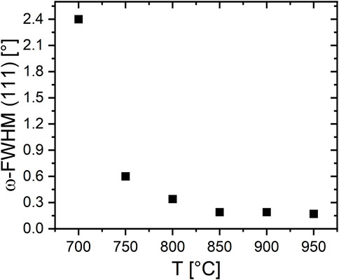
Figure 5. Dependence of the TiN XRD ω-FWHM on substrate temperature during SpE.
With the quality achieved, much better than for HfN, a successful growth of GaN on top can be in principle expected. When testing GaN overgrowth on TiN by MOVPE the direct growth on top fails due to poor seeding, similar to GaN on sapphire growth. Since doping of GaN is imperative to achieve a good conductivity for vertical devices a process using a low-temperature GaN seed and the GaN overgrowth, similar to a standard GaN-on-sapphire process is not preferred. Doping by Si will reduce the lateral growth rate required in this process for defect reduction. In addition, strain engineering is mandatory for thick crack-free GaN due to the thermal expansion coefficient mismatch between Si and GaN. We have therefore chosen a layer structure starting with 2 nm AlN:Si followed by two AlGaN:Si layers with decreasing Al-content and a Si-concentration in the upper 1018 cm-3 range. After this GaN:Si was grown on top. In-situ reflectometry already indicates that this approach is successful in regard of compressive strain (Figure 6A) on GaN during epitaxy, but it also leads to surface roughening. As in MOVPE processes, Si doping at high concentrations is known to lead to surface roughening and in addition promotes the loss of compression (Fritze et al., 2012; Nenstiel et al., 2015). We therefore switched to Ge as n-type dopant which can be doped at much higher concentrations (Fritze et al., 2012; Nenstiel et al., 2015) (Figure 6B). The surface roughness is reduced but still requires optimization. In XRD Θ-2Θ scans (Figure 6C) four separate peaks from TiN, the two AlGaN layers and GaN are visible with no visible difference for Si or Ge doped GaN. The 800 nm thick GaN:Ge layer results in XRD ω-FWHM values of 0.16° (576“) and 0.3° (1080“) for the (0002) and (10
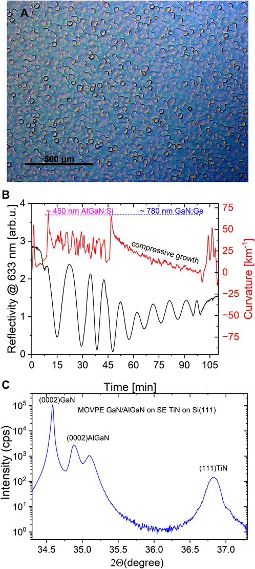
Figure 6. (A): Nomarski image of the sample surface. (B): in-situ measurement during AlGaN and GaN growth with the reflectivity change due to Fabry-Pérot interference and the curvature measurement demonstrating compressive growth of the GaN layer required for thick GaN device growth. (C): XRD Θ-2Θ scan of the whole structure showing the TiN(111) reflection and the (0002) reflections of the two AlGaN and the GaN layer.
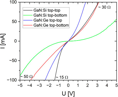
Figure 7. I–V current-voltage measurements between the bottom p-Si substrate and an In-dot on the sample surface as well as between two In-dots on the surface for samples where GaN was doped with Si or Ge. When using n-Si substrates better values can be expected.
Summary
In summary, we have investigated the growth of transition metal nitrides, namely, ScN, TiN, and HfN on Si substrates and the ternary compound AlScN on ScN on Si substrates by reactive magnetron sputter epitaxy. The epitaxial quality achieved for such layers is high although for AlScN on ScN still the pronounced columnar structure requires further improvement. In the case of TiN the crystalline quality is even better than the best AlN on Si layers, however still the morphology requires improvement to be better suited for group-III-nitride overgrowth. As potential application cases HfN has been demonstrated to switch the polarity of GaN grown on top and in the case of TiN we have shown the principle suitability for vertical devices on Si substrates.
Data availability statement
The raw data supporting the conclusions of this article will be made available by the authors, without undue reservation.
Author contributions
FH: Investigation, Writing–original draft, Writing–review and editing. CL: Investigation, Writing–original draft. JG: Investigation, Writing–review and editing. JB: Investigation, Writing–review and editing. MF: Investigation, Writing–review and editing. AD: Conceptualization, Funding acquisition, Project administration, Supervision, Writing–original draft, Writing–review and editing. RG: Supervision, Writing–review and editing. AS: Supervision, Writing–review and editing.
Funding
The author(s) declare that financial support was received for the research, authorship, and/or publication of this article. Most of the AlScN and HfN investigations and some of TiN were funded by the Deutsche Forschungsgemeinschaft (DFG) in the framework of the focused program GaNius (SPP2312) project #462722619 under contracts DA466/14-1 and FE1453/2-1 Some TiN investigations were funded by EU EFRE funding under contract ZS/2023/12/182333.
Acknowledgments
We like to thank the Deutsche Forschungsgemeinschaft (DFG) for funding part of the project in the framework of the focused program GaNius (SPP2312) project #462722619 under contracts DA466/14-1 FE1453/2-1 and by EU EFRE funding under contract ZS/2023/12/182333.
Conflict of interest
The authors declare that the research was conducted in the absence of any commercial or financial relationships that could be construed as a potential conflict of interest.
Generative AI statement
The author(s) declare that no Generative AI was used in the creation of this manuscript.
Publisher’s note
All claims expressed in this article are solely those of the authors and do not necessarily represent those of their affiliated organizations, or those of the publisher, the editors and the reviewers. Any product that may be evaluated in this article, or claim that may be made by its manufacturer, is not guaranteed or endorsed by the publisher.
References
Abid, I., Hamdaoui, Y., Mehta, J., Derluyn, J., and Medjdoub, F. (2022). Low buffer trapping effects above 1200 V in normally off GaN-on-Silicon field effect transistors. Micromachines 13, 1519. doi:10.3390/mi13091519
Armitage, R., Yang, Q., Feick, H., Gebauer, J., Weber, E. R., Shinkai, S., et al. (2002). Lattice-matched HfN buffer layers for epitaxy of GaN on Si. Appl. Phys. Lett. 81, 1450–1452. doi:10.1063/1.1501447
Chowdhury, S., Swenson, B. L., Wong, M. H., and Mishra, U. K. (2013). Current status and scope of gallium nitride-based vertical transistors for high-power electronics application. Semicond. Sci. Technol. 28, 074014. doi:10.1088/0268-1242/28/7/074014
Dadgar, A., Bläsing, J., Diez, A., Krost, A., Alam, A., and Heuken, M. (2000). Metalorganic chemical vapor phase epitaxy of crack-free GaN on Si (111) exceeding 1 µm in thickness. Jpn. J. Appl. Phys. 39 (L), 1183. doi:10.1143/jjap.39.l1183
Dadgar, A., Hörich, F., Borgmann, R., Bläsing, J., Schmidt, G., Veit, P., et al. (2022). Sputter epitaxy of AlN and GaN on Si(111). Phys. Stat. Sol. A 220, 2200609. doi:10.1002/pssa.202200609
Dadgar, A., and Krost, A. (2013). in Epitaxial growth and benefits of GaN on silicon in III-Nitride Semiconductors and their Modern Devices. Editor B. Gil (Oxford University Press).
Dadgar, A., Krost, A., Christen, J., Bastek, B., Bertram, F., Krtschil, A., et al. (2006). MOVPE growth of high-quality AlN. J. Cryst. Growth 297, 306–310. doi:10.1016/j.jcrysgro.2006.09.046
Dadgar, A., Schulze, F., Bläsing, J., Diez, A., Krost, A., Neuburger, M., et al. (2004). High-sheet-charge–carrier-density AlInN∕GaN field-effect transistors on Si(111). Appl. Phys. Lett. 85, 5400–5402. doi:10.1063/1.1828580
Fritze, S., Dadgar, A., Witte, H., Bügler, M., Rohrbeck, A., Bläsing, J., et al. (2012). High Si and Ge n-type doping of GaN doping - limits and impact on stress. Appl. Phys. Lett. 100, 122104. doi:10.1063/1.3695172
Hamdaoui, Y., Abid, I., Michler, S., Ziouche, K., and Medjdoub, F. (2024a). Compound semiconductor week May 2023. South Korea: Jeju.
Hamdaoui, Y., Vandenbroucke, S., Michler, S., Ziouche, K., Minjauw, M., Detavernier, C., et al. (2024b). Optimization of non-alloyed backside ohmic contacts to N-face GaN for fully vertical GaN-on-Silicon-Based power devices. Micromachines 15, 1157. doi:10.3390/mi15091157
Hörich, F., Borgmann, R., Bläsing, J., Schmidt, G., Veit, P., Bertram, F., et al. (2021). Demonstration of lateral epitaxial growth of AlN on Si (1 1 1) at low temperatures by pulsed reactive sputter epitaxy. J. Cryst. Growth 571, 126250. doi:10.1016/j.jcrysgro.2021.126250
Kanechika, M., Sugimoto, M., Soeima, N., Ueda, H., Ishiguro, O., Kodama, M., et al. (2007). Japan. J. Appl. Phys. 46, L503. doi:10.1143/JJAP.46.L503
Krause, S., Streicher, I., Waltereit, P., Kirste, L., Brückner, P., and Leone, S. (2023). AlScN/GaN HEMTs grown by metal-organic chemical vapor deposition with 8.4 W/mm output power and 48 % power-added efficiency at 30 GHz. IEEE Electron Device Lett. 44, 17–20. doi:10.1109/led.2022.3220877
Leone, S., Ligl, J., Manz, C., Kirste, L., Fuchs, T., Menner, H., et al. (2019). Metal-organic chemical vapor deposition of aluminum scandium nitride. Phys. Stat. Sol. RRL 14, 1900535. doi:10.1002/pssr.201900535
Ligl, J., Leone, S., Manz, C., Kirste, L., Doering, P., Fuchs, T., et al. (2020). Metalorganic chemical vapor phase deposition of AlScN/GaN heterostructures. J. Appl. Phys. 127, 195704. doi:10.1063/5.0003095
Mäenpää, M., Nicolet, M.-A., Suni, I., and Colgan, E. G. (1981). Contact resistivities of sputtered TiN and Ti TiN metallizations on solar-cell-type-silicon. Sol. Energy 27, 283–287. doi:10.1016/0038-092x(81)90060-8
Mihalic, S., Wade, E., Lüttich, C., Hörich, F., Sun, C., Fu, Z., et al. (2023). Structural properties and epitaxial relation of cubic rock salt ScxAl1-xN/ScN/Si. J. Appl. Phys. 134, 155107. doi:10.1063/5.0169741
Mohammad, S. N., Salvador, A. A., and Morkoc, H. (1995). Emerging gallium nitride based devices. Proc. IEEE 83, 1306–1355. doi:10.1109/5.469300
Nakamura, S., Senoh, M., and Mukai, T. (1993). P-GaN/N-InGaN/N-GaN double-heterostructure blue-light-emitting diodes. J. Appl. Phys. 32, L8. doi:10.1143/jjap.32.l8
Nenstiel, C., Bügler, M., Callsen, G., Nippert, F., Kure, T., Fritze, S., et al. (2015). Germanium - the superior dopant in n-type GaN. Phys. Stat. Sol. RRL 9, 716–721. doi:10.1002/pssr.201510278
Perry, A. J., Georgson, M., and Sproul, W. D. (1988). Variations in the reflectance of TiN, ZrN and HfN. Thin Solid Films 157, 255–265. doi:10.1016/0040-6090(88)90007-7
Pezzagna, S., Vennéguès, P., Grandjean, N., and Massies, J. (2004). Polarity inversion of GaN(0001) by a high Mg doping. J. Cryst. Growth 269, 249–256. doi:10.1016/j.jcrysgro.2004.05.067
Salamat, A., Hector, A. L., Gray, B. M., Kimber, S. A. J., Bouvier, P., and McMillan, P. F. (2013). Synthesis of tetragonal and orthorhombic polymorphs of Hf3N4 by high-pressure annealing of a prestructured nanocrystalline precursor. J. Am. Chem. Soc. 135, 9503–9511. doi:10.1021/ja403368b
Sproul, W. D. (1984). Hafnium nitride coatings prepared by very high rate reactive sputtering. Thin Solid Films 118, 279–284. doi:10.1016/0040-6090(84)90198-6
Streicher, I., Leone, S., Zhang, M., Slimani Tlemcani, T., Bah, M., Straňák, P., et al. (2024). Understanding interfaces in AlScN/GaN heterostructures. Adv. Funct. Mater. 34, 2403027. doi:10.1002/adfm.202403027
Weyher, J. L., Macht, L., Kamler, G., Borysiuk, J., and Grzegory, I. (2003). Characterization of GaN single crystals by defect-selective etching. Phys. Stat. Sol. C 0, 821–826. doi:10.1002/pssc.200306248
Keywords: sputter epitaxy, transition metal nitrides, group III-nitrides, x-ray diffraction, vertical GaN on Si electronics
Citation: Hörich F, Lüttich C, Grümbel J, Bläsing J, Feneberg M, Dadgar A, Goldhahn R and Strittmatter A (2025) Epitaxial growth of transition metal nitrides by reactive sputtering. Front. Mater. 12:1507123. doi: 10.3389/fmats.2025.1507123
Received: 07 October 2024; Accepted: 08 January 2025;
Published: 29 January 2025.
Edited by:
Stefano Leone, Fraunhofer IAF, GermanyReviewed by:
Appu Vengattoor Raghu, Vienna University of Technology, AustriaIsabel Streicher, National Research Council (CNR), Italy
Copyright © 2025 Hörich, Lüttich, Grümbel, Bläsing, Feneberg, Dadgar, Goldhahn and Strittmatter. This is an open-access article distributed under the terms of the Creative Commons Attribution License (CC BY). The use, distribution or reproduction in other forums is permitted, provided the original author(s) and the copyright owner(s) are credited and that the original publication in this journal is cited, in accordance with accepted academic practice. No use, distribution or reproduction is permitted which does not comply with these terms.
*Correspondence: Armin Dadgar, YXJtaW4uZGFkZ2FyQG92Z3UuZGU=