 Kapil Saha
 Pietro Simeoni
- ECE Department, NanoSI Institute, Northeastern University, Boston, MA, United States
This study reports on the characterization of a
1 Introduction
Piezoelectric and ferroelectric materials are critical for microacoustic devices in applications such as sensing (Muralt et al., 2009; Fawzy and Zhang, 2019), acoustic communication (Xue et al., 2024), and RF filtering (Muralt, 2008; Azarnaminy et al., 2024). Among the piezoelectric materials, Aluminum Nitride (AlN) is particularly of interest due to its high acoustic velocity (Tabrizian et al., 2009), high thermal conductivity (Tabrizian et al., 2009), and compatibility with complementary metal-oxide semiconductor (CMOS) processes (Haider et al., 2023). Nevertheless, the low piezoelectric coefficients of AlN have restricted its performance in applications that require high electromechanical coupling (Manna et al., 2018).
To overcome this trade-off, there have been significant research thrusts to increase the piezoelectric coupling of AlN by introducing additional elements in the crystal, with the notable success of scandium (Sc) doping, which significantly enhances both the piezoelectric and ferroelectric properties of the material and is currently being deployed for commercial applications (Wingqvist et al., 2010; Matloub et al., 2013; Olsson et al., 2020; Startt et al., 2023). This enhancement was first reported by researchers who demonstrated considerable improvements in the piezoelectric response of Sc-doped AlN thin films prepared by dual reactive co-sputtering (Akiyama et al., 2010; Kurz et al., 2019; Beaucejour et al., 2022). Ab-initio models and experimental results reported in literature (Tasnádi et al., 2010; Caro et al., 2015; Akiyama et al., 2009) indicate that Sc concentrations up to
Expanding upon this research, Jing et al. (Jing et al., 2022) performed a theoretical investigation utilizing density functional theory (DFT) simulations to explore the co-doping effect of Sc and B in AlN. Their findings indicated that the incorporation of a specific concentration of boron (B) into AlScN not only improves the piezoelectric stress coefficient
2 Experimental methods
AlScBN thin films were deposited on 200 mm Silicon (Si) (100) substrates using an Evatec® Clusterline-200 II magnetron sputtering system under high vacuum conditions, maintaining pressures around
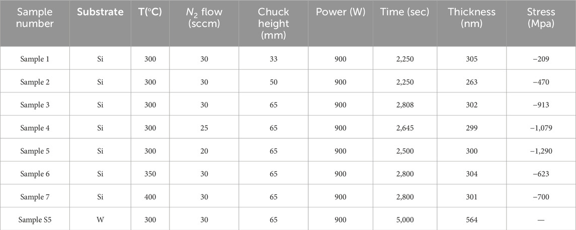
Table 1. Deposition parameters used for the sputtering process of AlScBN thin films.
A tungsten (W) layer was used as the bottom electrode on a 200 mm silicon (100) double-sided polished (DSP) substrate. Subsequently, a 564 nm-thick AlScBN thin film was deposited over the metal layer. To know the surface topology of this sample, roughness measurement was conducted utilizing a Park XE-7 Atomic Force Microscope (AFM) in non-contact mode. To facilitate the measurement of piezoelectric and ferroelectric responses, a 150 nm platinum (Pt) layer was deposited and patterned as the top electrode on the AlScBN film. The parallel-plate capacitors were patterned in circles and square shapes with different areas. Electrical access to the blanket bottom electrode was created by deliberately removing small portions of the piezoelectric surface through scratching. Indium (In) paste was applied to the scratched area to ensure proper electrical grounding of the bottom electrode. The piezoelectric properties of AlScBN were investigated utilizing an aixACCT Double-Beam Laser Interferometer (DBLI). The
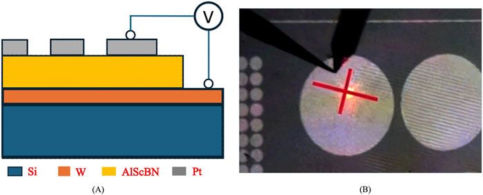
Figure 1. (A) Schematic cross-sectional view of the sample film stack; (B) top view of the AlScBN on W sample, showing patterned top electrode and aligned laser beam for displacement measurement.
3 Results and discussion
3.1 Stress optimization
For the stress optimization, AlScBN films deposited on Si (100) 200 mm substrates were examined. The stress data and thickness of the deposited films, obtained from the Ellipsometer measurements, are summarized in Table 1. According to the data reported in Table 1, it is notable that increasing the distance between the target and substrate can make the film more compressive. It is also evident that at constant temperature and target-substrate distance, the stress tends to be more compressive with decreasing order of
Figure 2 illustrates the film’s stress dependence on multiple process parameters, such as chuck height,
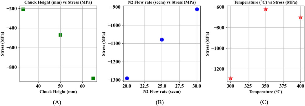
Figure 2. Stress dependence on process parameters: (A) target-to-substrate distance, (B)
3.2 Crystallographic orientation and crystallinity
The Gonio scan (2
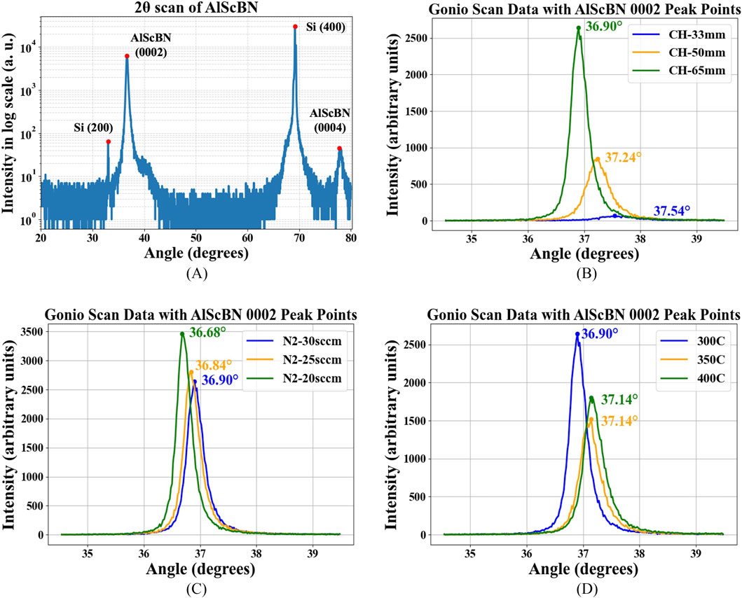
Figure 3. (A) XRD
The crystallinity of the deposited films was analyzed using the full width at half maximum (FWHM) of the ω scan (rocking curve) under various conditions, as shown in Figure 4. Figure 4A illustrates the
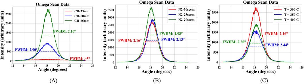
Figure 4. XRD
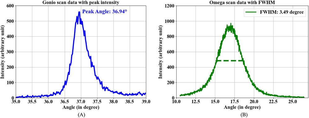
Figure 5. (A) 2
3.3 Film surface quality
The presence of abnormally oriented grains (AOGs) was observed using SEM in order to assess the surface quality of the films deposited on Si (100) substrates. According to reports, the density of the AOGs increases as the Sc content in the film increases (Fichtner et al., 2017; Assylbekova, 2022). The elevated concentration of AOGs in the film increases the film’s roughness, degrades the film quality, and reduces the piezoelectric response as well as the quality factor in piezoelectric acoustic resonators (Sandu et al., 2019; Liu et al., 2020). Figure 6 depicts the surface quality of thin films under different process conditions: Figure 6A shows the effect of chuck height, Figure 6B depicts the influence of
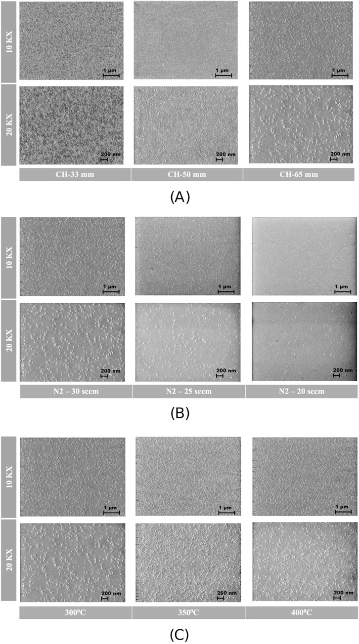
Figure 6. SEM visualization of film surface quality for films deposited at different (A) chuck heights, (B)
The SEM images were then analyzed using an advanced image recognition technique specifically developed for the quantitative evaluation of abnormally oriented grains (AOGs). This algorithm facilitates the accurate detection and measurement of grains on the substrate with pixel-level precision, enabling precise calculations of their average area and coverage Spagnuolo et al., 2024. Figure 7 presents the area distribution of the AOGs. A leftward shift in the peak of the curve indicates a higher percentage of smaller-sized AOGs. Narrow and sharp peaks suggest a higher probability of grains being of similar sizes, whereas a broader curve signifies the presence of AOGs with a wide range of different areas. The AOG area distribution curve provides quantitative support for observations made through the visual inspection of SEM images. The leftmost red curve corresponds to Sample 5, which was deposited at a temperature of 300°C, with a
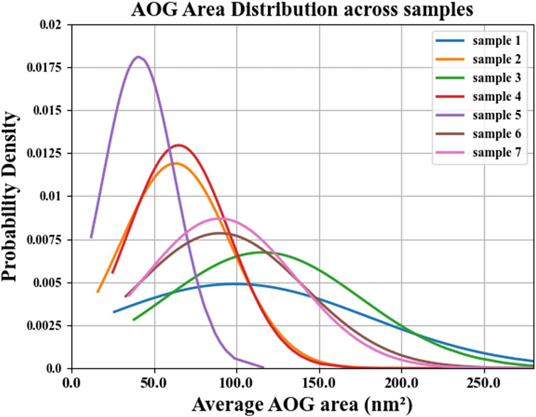
Figure 7. AOG area distribution curve for samples deposited on Si.
Considering the trade-off among the process parameters, an optimal deposition temperature of 300°C, accompanied by a
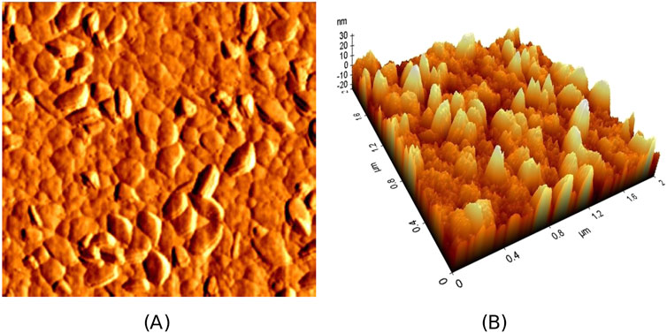
Figure 8. Surface imaging by AFM: (A) top-view surface of the AlScBN film deposited on W, and (B) 3D view of the surface.
3.4 Piezoelectric measurements
The longitudinal piezoelectric coefficient
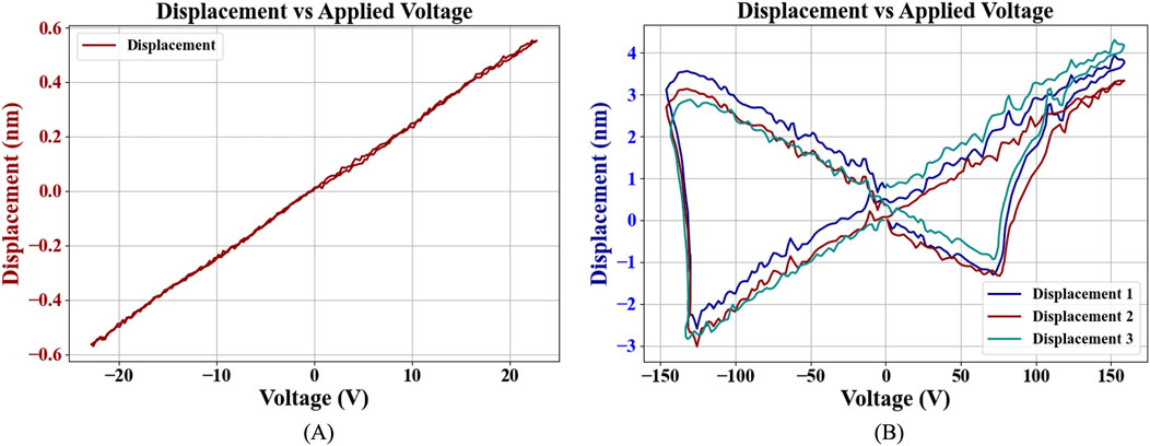
Figure 9. (A) Linear displacement proportional to the applied voltage below the coercive field, and (B) non-linear displacement with the applied voltage above the coercive field (Butterfly curve).
3.5 Ferroelectric measurements
Using the same experimental system (DBLI), Dynamic Hysteresis Measurement (DHM) was carried out to showcase the polarization switching, highlighting the remnant polarization
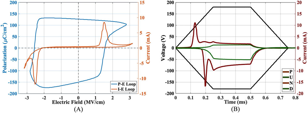
Figure 10. (A) Polarization and switching current with respect to electric field, showing remnant polarization and the coercive field (DHM); (B) Voltage-current plot with respect to time showing the polarization switching current peaks and leakage current (PUND).
Table 2 showcases a comparative analysis of the piezoelectric and ferroelectric properties of AlScBN, AlBN, and AlScN reported in the literature, along with the respective measuring techniques.
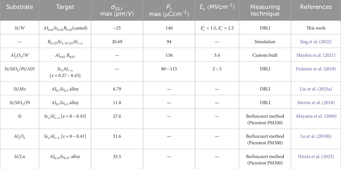
Table 2. Comparison table for piezoelectric (
4 Conclusion
The incorporation of Boron (B) into AlScN films was thought to stabilize the wurtzite phase at high Sc concentrations and close to the theoretical instability region of AlScN. A high piezoelectric response was measured, and the ferroelectric hysteresis of AlScBN indicates higher remnant polarization and lower coercive field than 43% doped ScAlN (Fichtner et al., 2020). DBLI measurements showed a longitudinal piezoelectric coefficient
Data availability statement
The raw data supporting the conclusions of this article will be made available by the authors upon request.
Author contributions
KS: Conceptualization, Data Curation, Formal Analysis, Investigation, Methodology, Validation, Visualization, Writing–original draft, Writing–review and editing. PS: Conceptualization, Data curation, Formal Analysis, Investigation, Methodology, Project Administration, Supervision, Validation, Writing–review and editing. LC: Project administration, Software, Supervision, Writing–review and editing. MR: Conceptualization, Funding acquisition, Project Administration, Supervision, Writing–review and editing.
Funding
The author(s) declare that no financial support was received for the research and/or publication of this article.
Acknowledgments
The authors thank the Kostas Nanoscale Technology and Manufacturing Research Center cleanroom facility and it’s staff for providing the support and required infrastructure for this experimental study.
Conflict of interest
The authors confirm that the research was conducted in the absence of any commercial or financial relationships that could be construed as a potential conflict of interest.
Generative AI statement
The author(s) declare that no Generative AI was used in the creation of this manuscript.
Publisher’s note
All claims expressed in this article are solely those of the authors and do not necessarily represent those of their affiliated organizations, or those of the publisher, the editors and the reviewers. Any product that may be evaluated in this article, or claim that may be made by its manufacturer, is not guaranteed or endorsed by the publisher.
References
Akiyama, M., Kano, K., and Teshigahara, A. (2009). Influence of growth temperature and scandium concentration on piezoelectric response of scandium aluminum nitride alloy thin films. Appl. Phys. Lett. 95, 162107. doi:10.1063/1.3251072
Akiyama, M., Tabaru, T., Nishikubo, K., Teshigahara, A., and Kano, K. (2010). Preparation of scandium aluminum nitride thin films by using scandium aluminum alloy sputtering target and design of experiments. J. Ceram. Soc. Jpn. 118, 1166–1169. doi:10.2109/jcersj2.118.1166
Assylbekova, M. (2022). Aluminum nitride and scandium-doped aluminum nitride materials and devices for beyond 6 GHz communication. Ph.D. thesis. Copyright - Database copyright ProQuest LLC; ProQuest does not claim copyright in the individual underlying works.
Azarnaminy, A. F., Ou, M., and Mansour, R. R. (2024). Pcm-based reconfigurable acoustic resonators and filters: for potential use in rf front-end applications. IEEE Microw. Mag. 25, 48–67. doi:10.1109/MMM.2023.3332286
Beaucejour, R., Roebisch, V., Kochhar, A., Moe, C. G., Hodge, M. D., and Olsson, R. H. (2022). Controlling residual stress and suppression of anomalous grains in aluminum scandium nitride films grown directly on silicon. J. Microelectromechanical Syst. 31, 604–611. doi:10.1109/JMEMS.2022.3167430
Caro, M. A., Zhang, S., Riekkinen, T., Ylilammi, M., Moram, M. A., Lopez-Acevedo, O., et al. (2015). Piezoelectric coefficients and spontaneous polarization of scaln. J. Phys. Condens. Matter 27, 245901. doi:10.1088/0953-8984/27/24/245901
Deng, B., Zhang, Y., and Shi, Y. (2024). Examining the ferroelectric characteristics of aluminum nitride-based thin films. J. Am. Ceram. Soc. 107, 1571–1581. doi:10.1111/jace.19540
Fawzy, A., and Zhang, M. (2019). “Piezoelectric thin film materials for acoustic mems devices,” in 2019 6th international conference on advanced control circuits and systems (ACCS) 2019 5th international conference on new paradigms in electronics information Technology (PEIT), 82–86. doi:10.1109/ACCS-PEIT48329.2019.9062834
Fichtner, S., Lofink, F., Wagner, B., Schönweger, G., Kreutzer, T.-N., Petraru, A., et al. (2020). “Ferroelectricity in alscn: switching, imprint and sub-150 nm films,” in 2020 joint conference of the IEEE international frequency control symposium and international symposium on applications of ferroelectrics (IFCS-isaf), 1–4.
Fichtner, S., Wolff, N., Krishnamurthy, G., Petraru, A., Bohse, S., Lofink, F., et al. (2017). Identifying and overcoming the interface originating c-axis instability in highly Sc enhanced AlN for piezoelectric micro-electromechanical systems. J. Appl. Phys. 122, 035301. doi:10.1063/1.4993908
Fichtner, S., Wolff, N., Lofink, F., Kienle, L., and Wagner, B. (2019). Alscn: a iii-v semiconductor based ferroelectric. J. Appl. Phys. 125, 114103. doi:10.1063/1.5084945
Fields, S. S., Jaszewski, S. T., Lenox, M. K., and Ihlefeld, J. F. (2023). Asymmetric electrode work function customization via top electrode replacement in ferroelectric and field-induced ferroelectric hafnium zirconium oxide thin films. Adv. Mater. Interfaces 10, 2202232. doi:10.1002/admi.202202232
Gremmel, M., and Fichtner, S. (2024). The interplay between imprint, wake-up, and domains in ferroelectric al0.70sc0.30n. J. Appl. Phys. 135, 204101. doi:10.1063/5.0197111
Gund, V., Davaji, B., Lee, H., Casamento, J., Xing, H. G., Jena, D., et al. (2021). “Towards realizing the low-coercive field operation of sputtered ferroelectric ScxAl1-xN,” in 2021 21st international conference on solid-state sensors, actuators and microsystems (transducers), 1064–1067.
Haider, S. T., Shah, M. A., Lee, D.-G., and Hur, S. (2023). A review of the recent applications of aluminum nitride-based piezoelectric devices. IEEE Access 11, 58779–58795. doi:10.1109/ACCESS.2023.3276716
Hayden, J., Hossain, M. D., Xiong, Y., Ferri, K., Zhu, W., Imperatore, M. V., et al. (2021). Ferroelectricity in boron-substituted aluminum nitride thin films. Phys. Rev. Mat. 5, 044412. doi:10.1103/PhysRevMaterials.5.044412
Hirata, K., Niitsu, K., Anggraini, S. A., Kageura, T., Uehara, M., Yamada, H., et al. (2025). Enhancing the piezoelectric performance of nitride thin films through interfacial engineering. Mater. Today. doi:10.1016/j.mattod.2024.12.011
Huang, Z., Zhang, Q., Corkovic, S., Dorey, R., and Whatmore, R. W. (2006). Comparative measurements of piezoelectric coefficient of pzt films by berlincourt, interferometer, and vibrometer methods. IEEE Trans. Ultrasonics, Ferroelectr. Freq. Control 53, 2287–2293. doi:10.1109/TUFFC.2006.175
Jing, H., Wang, Y., Wen, Q., Cai, X., Liu, K., Li, W., et al. (2022). Large piezoelectric and elastic properties in B and Sc codoped wurtzite AlN. J. Appl. Phys. 131, 245108. doi:10.1063/5.0090501
Kurz, N., Ding, A., Urban, D. F., Lu, Y., Kirste, L., Feil, N. M., et al. (2019). Experimental determination of the electro-acoustic properties of thin film alscn using surface acoustic wave resonators. J. Appl. Phys. 126, 075106. doi:10.1063/1.5094611
Liu, C., Chen, B., Li, M., Zhu, Y., and Wang, N. (2020). “Evaluation of the impact of abnormally orientated grains on the performance of scaln-based laterally coupled alternating thickness (lcat) mode resonators and lamb wave mode resonators,” in 2020 IEEE international ultrasonics symposium (IUS), 1–3. doi:10.1109/IUS46767.2020.9251507
Liu, C., Varghese, B., Liu, P. P., Lin, H., Li, M., and Zhu, Y. (2023a). “Measurement and analysis of longitudinal and transversal effective piezoelectric coefficients 100 nm-500 nm Sc0.3Al0.7N films,” in 2023 IEEE international ultrasonics symposium (IUS), 1–4. doi:10.1109/IUS51837.2023.10306779
Liu, F., Fina, I., Bertacco, R., and Fontcuberta, J. (2016). Unravelling and controlling hidden imprint fields in ferroelectric capacitors. Sci. Rep. 6, 25028. doi:10.1038/srep25028
Liu, W., Ko, J., and Zhu, W. (2001). Asymmetric switching behavior of ni/pb1.1(zr0.3ti0.7)o3/pt thin films. Mater. Lett. 49, 122–126. doi:10.1016/S0167-577X(00)00354-2
Liu, X., Ting, J., He, Y., Fiagbenu, M. M. A., Zheng, J., Wang, D., et al. (2022). Reconfigurable compute-in-memory on field-programmable ferroelectric diodes. Nano Lett. 22, 7690–7698. doi:10.1021/acs.nanolett.2c03169
Liu, Z., Wang, X., Ma, X., Yang, Y., and Wu, D. (2023b). Doping effects on the ferroelectric properties of wurtzite nitrides. Appl. Phys. Lett. 122, 122901. doi:10.1063/5.0145818
Lo, V. C., and Chen, Z. J. (2002). Simulation of the effects of space charge and Schottky barriers on ferroelectric thin film capacitor using landau khalatnikov theory. IEEE Trans. Ultrasonics, Ferroelectr. Freq. Control 49, 980–986. doi:10.1109/TUFFC.2002.1020168
Lü, T., and Cao, W. (2003). Influence of imperfect surface on properties of ferroelectric thin film. Microelectron. Eng. 66, 818–824. doi:10.1016/S0167-9317(02)01005-5
Lu, Y., Reusch, M., Kurz, N., Ding, A., Christoph, T., Kirste, L., et al. (2018a). Surface morphology and microstructure of pulsed dc magnetron sputtered piezoelectric aln and alscn thin films. Phys. status solidi (a) 215, 1700559. doi:10.1002/pssa.201700559
Lu, Y., Reusch, M., Kurz, N., Ding, A., Christoph, T., Prescher, M., et al. (2018b). Elastic modulus and coefficient of thermal expansion of piezoelectric Al1−xScxN (up to x = 0.41) thin films. Apl. Mater. 6, 076105. doi:10.1063/1.5040190
Manna, S., Talley, K. R., Gorai, P., Mangum, J. S., Zakutayev, A., Brennecka, G. L., et al. (2018). Enhanced piezoelectric response of aln via crn alloying. Phys. Rev. Appl. 9, 034026. doi:10.1103/physrevapplied.9.034026
Matloub, R., Hadad, M., Mazzalai, A., Chidambaram, N., Moulard, G., Sandu, C. S., et al. (2013). Piezoelectric Al1−xScxN thin films: a semiconductor compatible solution for mechanical energy harvesting and sensors. Appl. Phys. Lett. 102. doi:10.1063/1.4800231
Mertin, S., Heinz, B., Mazzalar, A., Schmitz-Kempen, T., Tiedke, S., and Pensala, T. (2018). High-volume production and non-destructive piezo-property mapping of 33In 2018 IEEE International Ultrasonics Symposium (IUS). 1–4. doi:10.1109/ULTSYM.2018.8580120
Michaelson, H. B. (1977). The work function of the elements and its periodicity. J. Appl. Phys. 48, 4729–4733. doi:10.1063/1.323539
Muralt, P. (2008). Recent progress in materials issues for piezoelectric MEMS. J. Am. Ceram. Soc. 91, 1385–1396. doi:10.1111/j.1551-2916.2008.02421.x
Muralt, P., Polcawich, R. G., and Trolier-McKinstry, S. (2009). Piezoelectric thin films for sensors, actuators, and energy harvesting. MRS Bull. 34, 658–664. doi:10.1557/mrs2009.177
Olsson, R. H., Tang, Z., and D’Agati, M. (2020). “Doping of aluminum nitride and the impact on thin film piezoelectric and ferroelectric device performance,” in 2020 IEEE custom integrated circuits conference (CICC), 1–6.
Pirro, M., Herrera, B., Assylbekova, M., Giribaldi, G., Colombo, L., and Rinaldi, M. (2021). “Characterization of dielectric and piezoelectric properties of ferroelectric alscn thin films,” in 2021 IEEE 34th international conference on micro electro mechanical systems (MEMS), 646–649. doi:10.1109/MEMS51782.2021.9375427
Pirro, M., Zhao, X., Herrera, B., Simeoni, P., and Rinaldi, M. (2022). Effect of substrate-rf on sub-200 nm al0.7sc0.3n thin films. Micromachines 13, 877. doi:10.3390/mi13060877
Saha, K. (2023). Characterization of scandium-doped aluminum nitride thin films for bulk acoustic wave resonators. Politecnico di Torino: Ph.D. thesis.
Sandu, C. S., Parsapour, F., Mertin, S., Pashchenko, V., Matloub, R., LaGrange, T., et al. (2019). Abnormal grain growth in AlScN thin films induced by complexion formation at crystallite interfaces. Phys. status solidi (a) 216, 1800569. doi:10.1002/pssa.201800569
Sivaramakrishnan, S., Mardilovich, P., Mason, A., Roelofs, A., Schmitz-Kempen, T., and Tiedke, S. (2013). Electrode size dependence of piezoelectric response of lead zirconate titanate thin films measured by double beam laser interferometry. Appl. Phys. Lett. 103, 132904. doi:10.1063/1.4821948
Sivaramakrishnan, S., Mardilovich, P., Schmitz-Kempen, T., and Tiedke, S. (2018). Concurrent wafer-level measurement of longitudinal and transverse effective piezoelectric coefficients (d33,f and e31,f) by double beam laser interferometry. J. Appl. Phys. 123, 014103. doi:10.1063/1.5019568
Spagnuolo, L., Colombo, L., Gubinelli, W., Saha, K., Simeoni, P., and Rinaldi, M. (2024). “An image recognition technique for the quantitative analysis of abnormally oriented grains in advanced piezoelectric material,” in 2024 IEEE ultrasonics, ferroelectrics, and frequency control joint symposium (UFFC-js), 1–3. doi:10.1109/UFFC-JS60046.2024.10794029
Startt, J., Quazi, M., Sharma, P., Vazquez, I., Poudyal, A., Jackson, N., et al. (2023). Unlocking AlN piezoelectric performance with earth-abundant dopants. Adv. Electron. Mater. 9, 2201187. doi:10.1002/aelm.202201187
Stoney, G. G. (1909). The tension of metallic films deposited by electrolysis. Proc. R. Soc. Lond. Ser. A, Contain. Pap. a Math. Phys. Character 82, 172–175.
Tabrizian, R., Rais-Zadeh, M., and Ayazi, F. (2009). “Effect of phonon interactions on limiting the f.q product of micromechanical resonators,” in Transducers 2009 - 2009 international solid-state sensors, actuators and microsystems conference, 2131–2134. doi:10.1109/SENSOR.2009.5285627
Tan, G., and Li, W. (2015). Ferroelectricity and ferromagnetism of m-type lead hexaferrite. J. Am. Ceram. Soc. 98, 1812–1817. doi:10.1111/jace.13530
Tan, X., Xu, Z., Liu, X., and Fan, Z. H. (2017). Double hysteresis loops at room temperature in nanbo3-based lead-free antiferroelectric ceramics. Mater. Res. Lett. 6, 159–164. doi:10.1080/21663831.2017.1419994
Tasnádi, F., Alling, B., Höglund, C., Wingqvist, G., Birch, J., Hultman, L., et al. (2010). Origin of the anomalous piezoelectric response in wurtzite scxal1−xN alloys. Phys. Rev. Lett. 104, 137601. doi:10.1103/PhysRevLett.104.137601
Tholander, C., Tasnádi, F., Abrikosov, I. A., Hultman, L., Birch, J., and Alling, B. (2015). Large piezoelectric response of quaternary wurtzite nitride alloys and its physical origin from first principles. Phys. Rev. B 92, 174119. doi:10.1103/PhysRevB.92.174119
Wang, D., Zheng, J., Tang, Z., D’Agati, M., Gharavi, P. S. M., Liu, X., et al. (2020). “Ferroelectric c-axis textured aluminum scandium nitride thin films of 100 nm thickness,” in 2020 joint conference of the IEEE international frequency control symposium and international symposium on applications of ferroelectrics (IFCS-isaf), 1–4.
Wingqvist, G., Tasnádi, F., Žukauskaitedot;, A., Birch, J., Arwin, H., and Hultman, L. (2010). Increased electromechanical coupling in w−ScxAl1−xN. Appl. Phys. Lett. 97. doi:10.1063/1.3489939
Xue, Y., Liu, Y., Zhou, C., and Zhang, X. Y. (2024). Acoustic wave devices based on piezoelectric/ferroelectric thin films for high-frequency communication systems and sensing applications. Ceram. Int. 50, 52051–52058. doi:10.1016/j.ceramint.2024.03.212
Yassine, M., Nair, A., Fammels, J., Wade, E., Fu, Z., Yassine, A., et al. (2022). Influence of structural properties on the ferroelectric behavior of hexagonal alscn. J. Appl. Phys. 132, 114101. doi:10.1063/5.0103578
Zhu, W., Hayden, J., He, F., Yang, J., Tipsawat, P., Hossain, M. D., et al. (2021). Strongly temperature dependent ferroelectric switching in aln, al1-xscxn, and al1-xbxn thin films. Appl. Phys. Lett. 119. doi:10.1063/5.0057869
Keywords: piezoelectricity, ferroelectricity, MEMS, thin films, sputtering, AlScBN
Citation: Saha K, Simeoni P, Colombo L and Rinaldi M (2025) Piezoelectric and ferroelectric measurements on casted target-deposited N thin films. Front. Mater. 12:1567614. doi: 10.3389/fmats.2025.1567614
Received: 27 January 2025; Accepted: 04 March 2025;
Published: 02 April 2025.
Edited by:
Stefano Leone, Fraunhofer IAF, GermanyReviewed by:
Georg Schönweger, University of Kiel, GermanyYunfei He, University of Pennsylvania, United States
Copyright © 2025 Saha, Simeoni, Colombo and Rinaldi. This is an open-access article distributed under the terms of the Creative Commons Attribution License (CC BY). The use, distribution or reproduction in other forums is permitted, provided the original author(s) and the copyright owner(s) are credited and that the original publication in this journal is cited, in accordance with accepted academic practice. No use, distribution or reproduction is permitted which does not comply with these terms.
*Correspondence: Kapil Saha, c2FoYS5rQG5vcnRoZWFzdGVybi5lZHU=